This is an old revision of the document!
Check out our full list of Verilog based projects!
Verilog® HDL: Project 2
Using switches to control LEDs
Project Overview
The goal of this project is to take the simple example from Project 1 and program our FPGA with it so that we can control a single LED with a single switch. Then, we'll take the same program and expand it to have multiple switches control multiple LEDs. Brave users will be challenged (with some guidance) at the end to do the same thing with some external components. If you have not already installed Vivado, you can find a guide to do so here. If you are hoping for a Project 0 where you learn how to navigate the Vivado interface in the first place, we highly recommend the Getting Started with Vivado Guide.
A list of the previous projects can be found here.
This project presumes you are using an FPGA development board that has external slide switches and LEDs built into the board, much like the Digilent system boards. However, the project can be easily modified to accommodate different types of external inputs (buttons instead of switches) or to use external I/O components rather than embedded components. If you have any questions after reading through the project, please feel free to post them on the Digilent Forum where an engineer will be happy to assist you.
Some Background Information
The digital circuit we are building from Project 1 is called led_sw. With this project, the FPGA is receiving an input signal, in this case from an embedded switch, that can be logic high, '1', or logic low, '0'. The input is then passed directly to an embedded LED that shows the corresponding logic by being “on” (a logic high) or “off” (a logic low). Both the embedded switch and LED are connected to their own ports on the FPGA and are specified in the constraint file (for Vivado, this is the XDC file)
Relooking at the Simple Example HDL
The code shown in the Simple Example from Project 1 that we will break down was as follows:
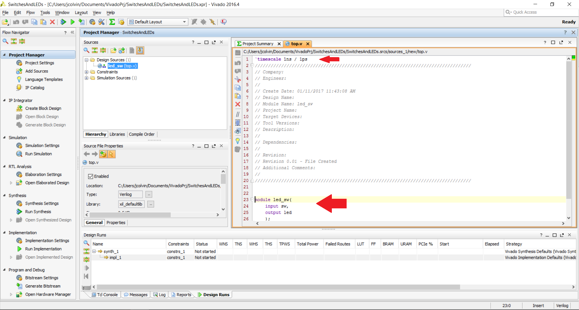
'timescale 1ns/1ps

module led_sw(
output led,
input sw
);
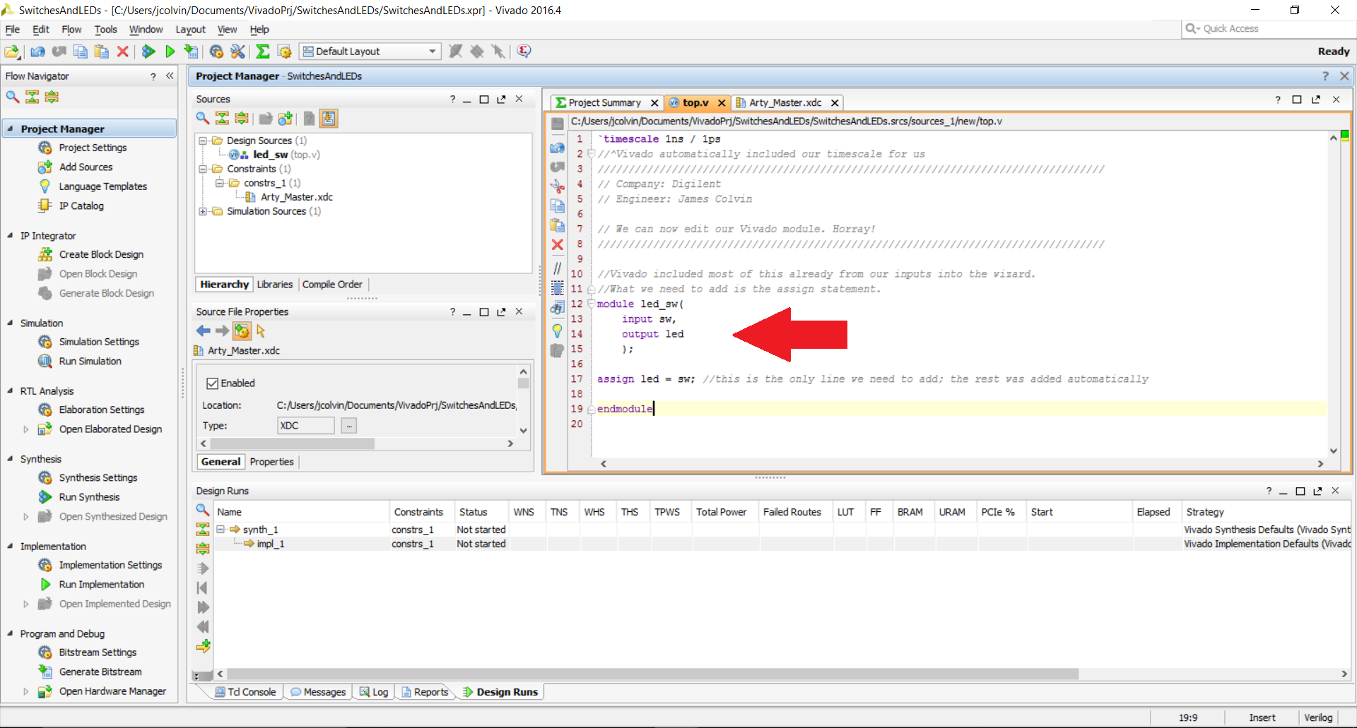
assign led = sw;

endmodule
The timescale portion 'timescale 1ns/1ps provides a base time length followed by a minimum time resolution. Generally speaking, this is only used during simulation and if delays are specifically implemented into the HDL, of which we are doing neither, but is a required part of Verilog modules nevertheless.
The module portion
module led_sw(
output led,
input sw
);
names and defines the number of inputs and outputs that we are creating on our custom “black box” (so-to-speak).
The assign portion assign led = sw; defines what our “black box” actually does. Multiple assign statements can be used as needed, as well as other ways of defining what our “black box” does (which we will get to in a later tutorial).
The endmodule is the keyword that signals the end of us defining what our module (our black box) does. Other modules could then be created with their own set of inputs and outputs, assign statements, and of course endmodule's.
But enough with the review, let's make our project!
Programming our FPGA
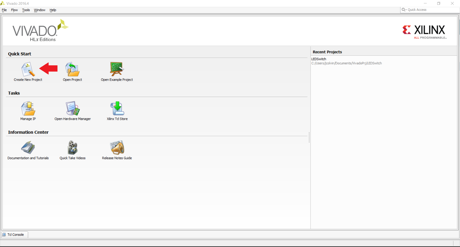
If you haven't already done so, go ahead and open up Vivado to the first screen and click on the “Create New Project” button. If you've gone through the Getting Started with Vivado Guide already, a lot of this will be very familiar to you (or near identical). You can follow along if you like, or if you feel that you can get your board programmed by yourself without the guide, feel free to do so (just to confirm you've got it right), and then jump down to the multiple switches and LEDs section.
On the opening screen, click on the “Create New Project” button.
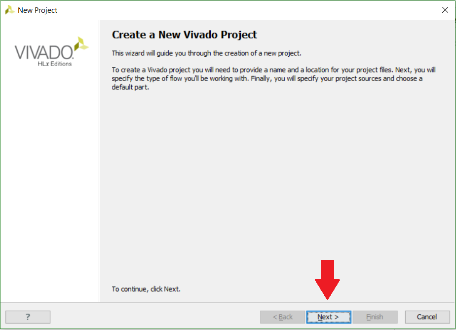
You'll then encounter some friendly instructions from Xilinx on how to create a new project. Click “Next”.
Here, we'll name our project and choose where to save our project file on our computer. It is critical that no spaces are used in either the name of the project or the file path that project is saved in; Vivado notoriously has problems with spaces, so using underscores or camelCase is recommended. It is also recommended to keep the file names and file paths relatively short so that character limits are not accidentally reached (maximum of 256 characters for a Windows operating system). Click “Next”.

Choose create a RTL (Register Transfer Level) project and keep the box unchecked so that we can specify sources for our project. Click “Next”.

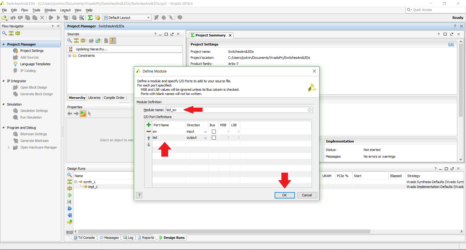
Click “Create file” to add our Verilog module.

In the window that pops up, keep the file type as Verilog and name your Verilog module. A commonly used name for modules, especially ones that call and use other modules, is “top”. We'll keep the file saved within our project file (as determined by Vivado). Click “OK”.

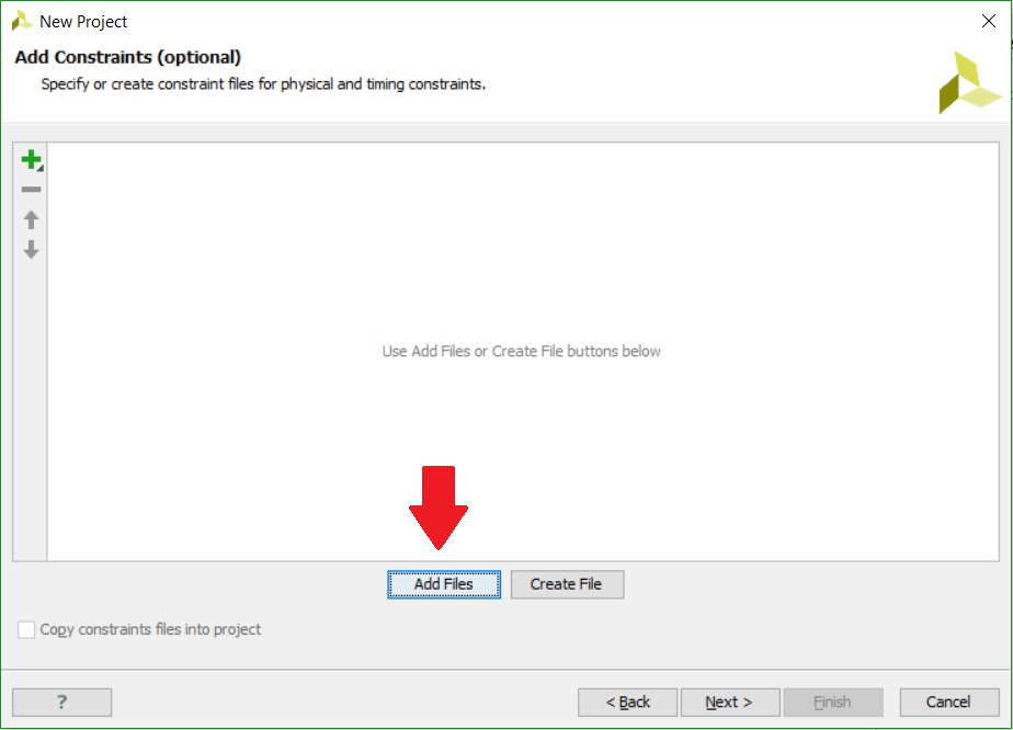
After clicking next on the IP cores since we don't have any to add, click “Add Files” on the Add Constraints page. Digilent boards have a master XDC (Xilinx Design Constraints) file available on their Wiki pages. Since I am using the Arty, I used the Master XDC available on it's Resource Center on the right hand side under “Design Resources” and saved mine to a convenient location on my computer.
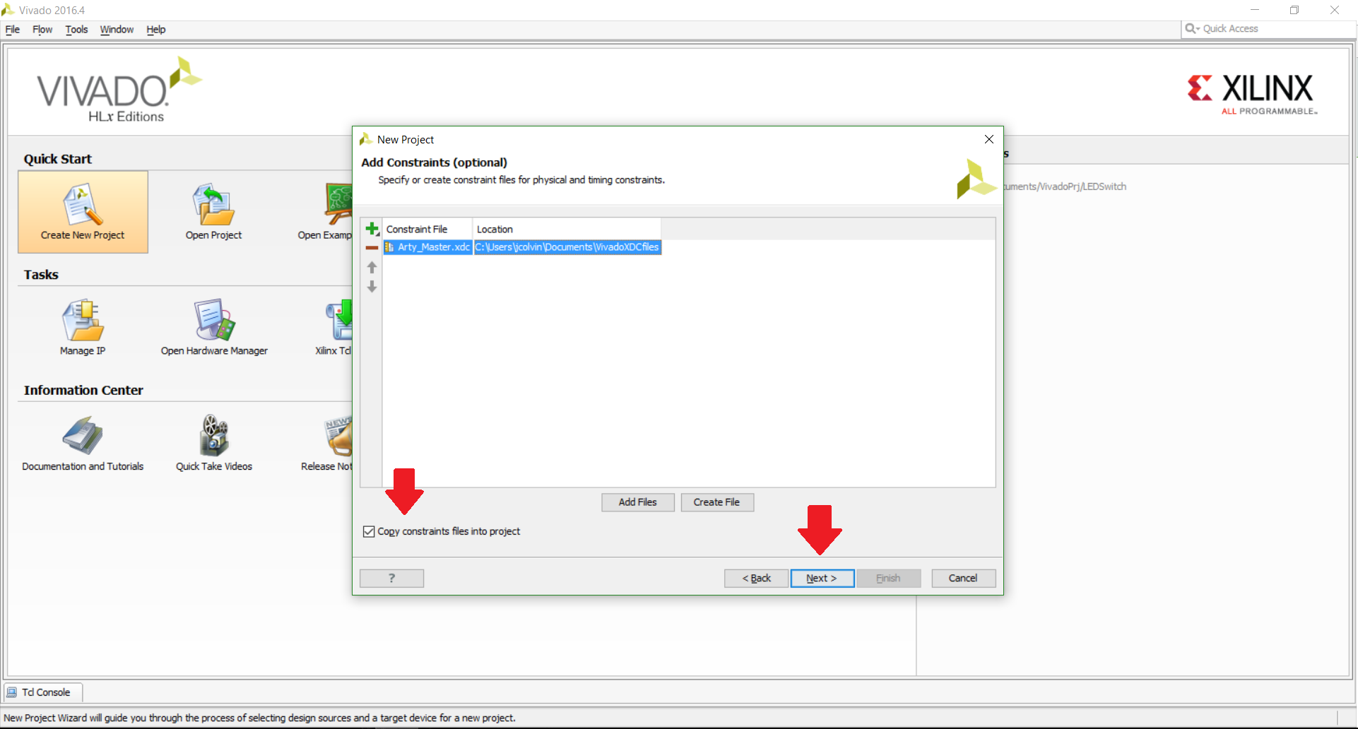
You'll get the opportunity to browse to your XDC file, which I happened to save in a folder that I named VivadoXDCfiles. Click “OK”.

Make sure you have the “Copy constraints files into project” button checked; this ensures you later edit a copy of the master xdc, rather than the original file. Then click “Next”.
Here you will want to select the FPGA that you are using to ensure that Vivado designs and programs the hardware correctly. You can either search by FPGA part number, or you can select your board from the “Boards” tab if you have a board file available. Digilent has board files available for each of their boards on GitHub; you can follow a tutorial on how to get them installed on your computer here. Once you have chosen the appropriate FPGA part (or board), click “Next”.


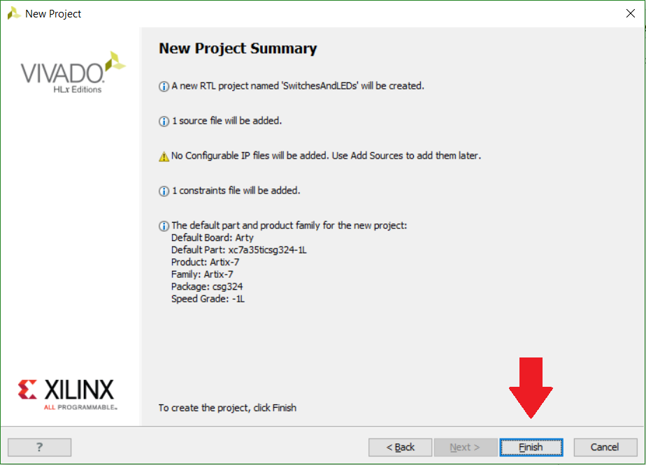
Confirm that your project has what you want to have (at least initially) and click “Finish”.
edit our constraints file
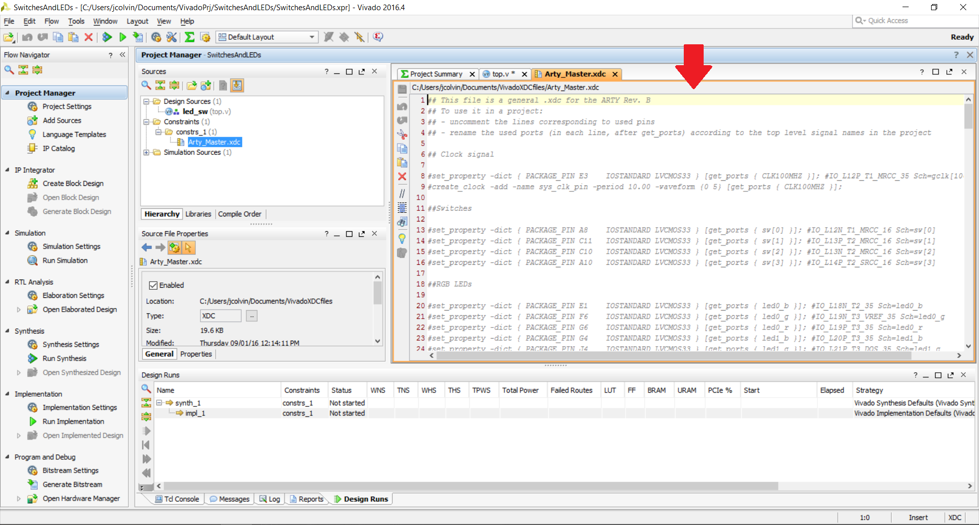
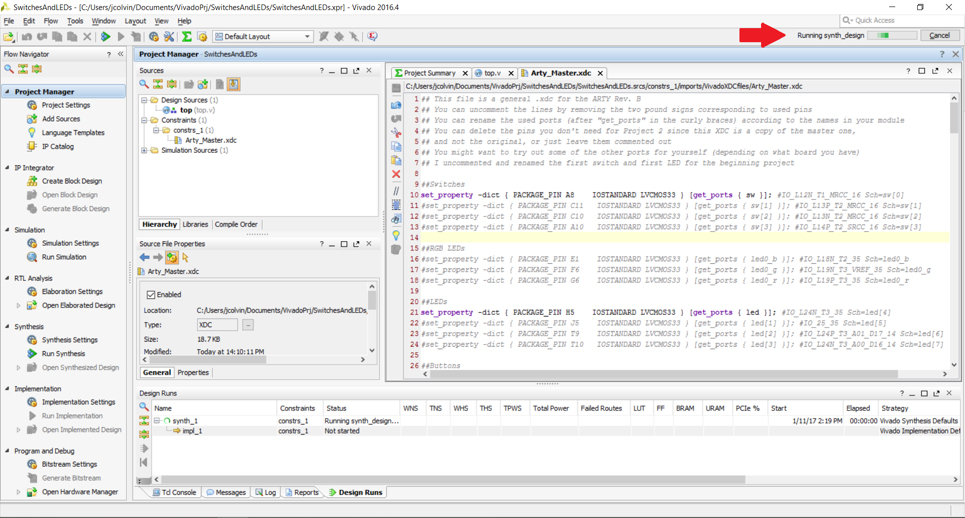
choose synthesis options; This can take awhile since Vivado processes a ton of things hidden to the user and works with the entire FPGA and not just what we are utilizing, so you'll probably want to maximize the number of jobs (computer cores Vivado is allowed to use) unless you plan to be doing a lot of other things simultaneously. For some of the larger projects we get into (which are still examples in the end) the synthesizing, implementing, and generating bitstream procedure can take upwards of 30 minutes if your computer isn't very fast.

synthesis running (about 30 seconds for me with 4 cores on an SSD)
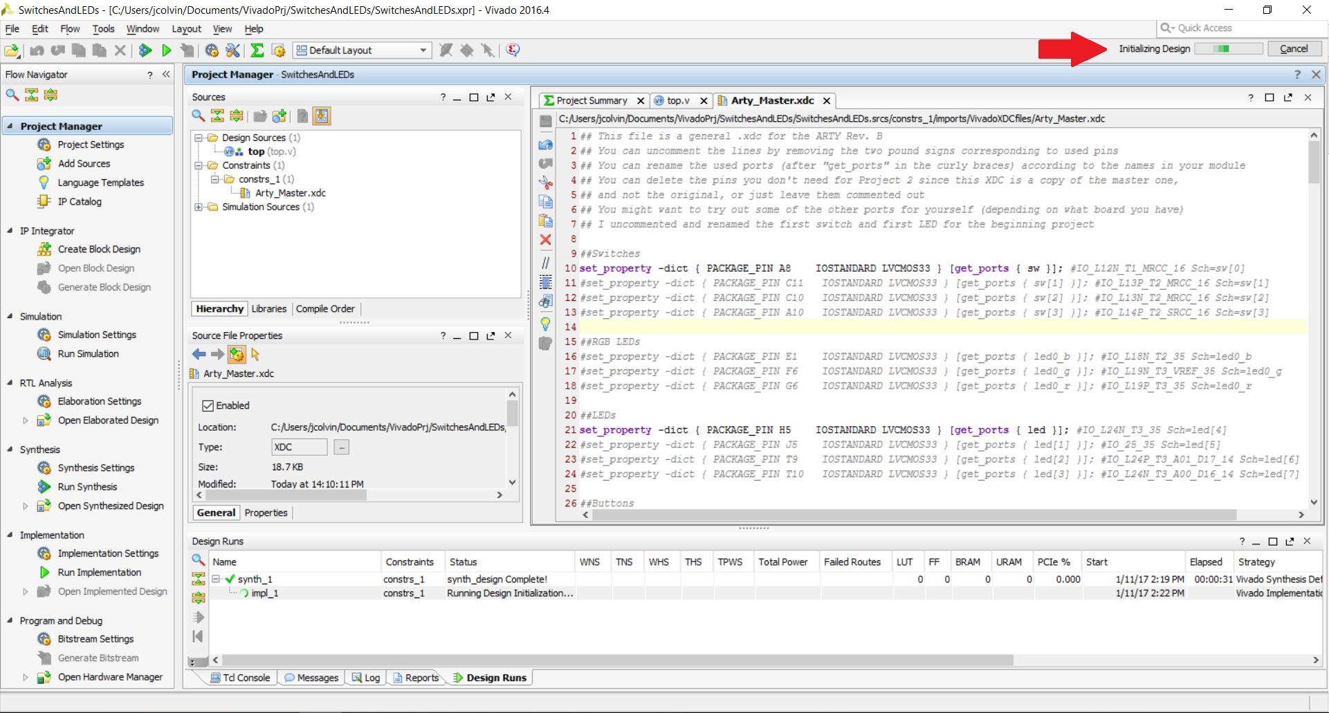
click run implementation on the wizard that pops up, can choose how many cores you use again if you haven't clicked the don't show this dialog again.

implementation running (45 seconds for me with 4 cores on an SSD)
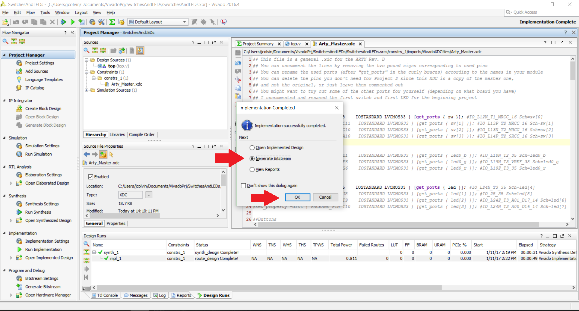
click generate bitstream on the wizard (don't necessarily want to click the “don't show this dialog again” here because if you are designing something on your own, you may want to just check to see if something got that far in the process or if theres already an error, not bother generating a bitstream for it), choose number of jobs/cores again
generate bitstream running (30 seconds for me with 4 cores on an SSD)
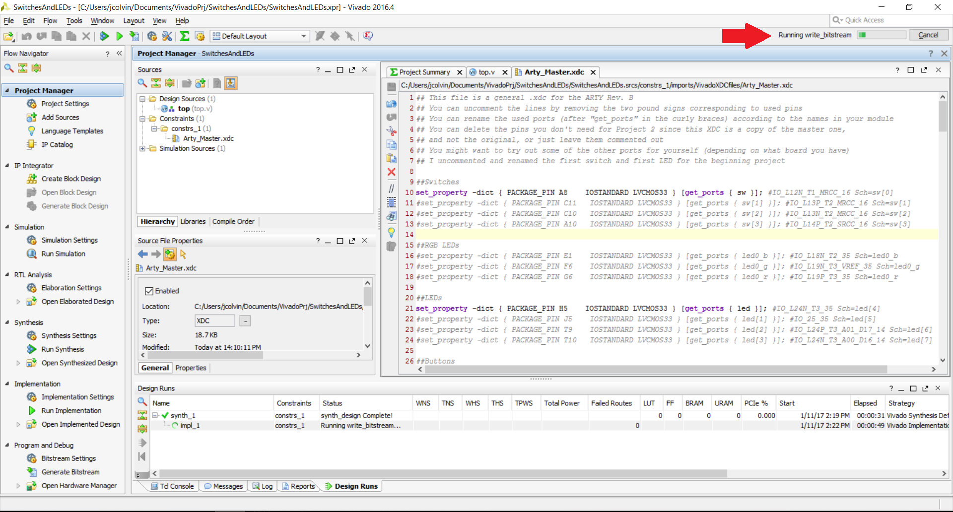
click open hardware manager on the wizard and then click ok.

if your FPGA is not connected already, you'll see a “no hardware target is open” message at the top.

You'll be able to click the “open target” screen and choose auto connect if you have connected your FPGA (make sure the power LEDs on the FPGA turn on when you connect it to your computer via the micro USB cable (if you are using a Digilent board)

You'll then be asked to choose the bitstream file (we don't have a debug core in our code, so we won't put anything in that field)

The bitstream file itself is a little unintuitive to find. You can find it by opening up the folder where you told Vivado to initially save your project, go to <projectName>.runs, then impl_1, and then choose the .bit that you see. I named my overall Verilog module top.v, so the bit file is top.bit. then click ok
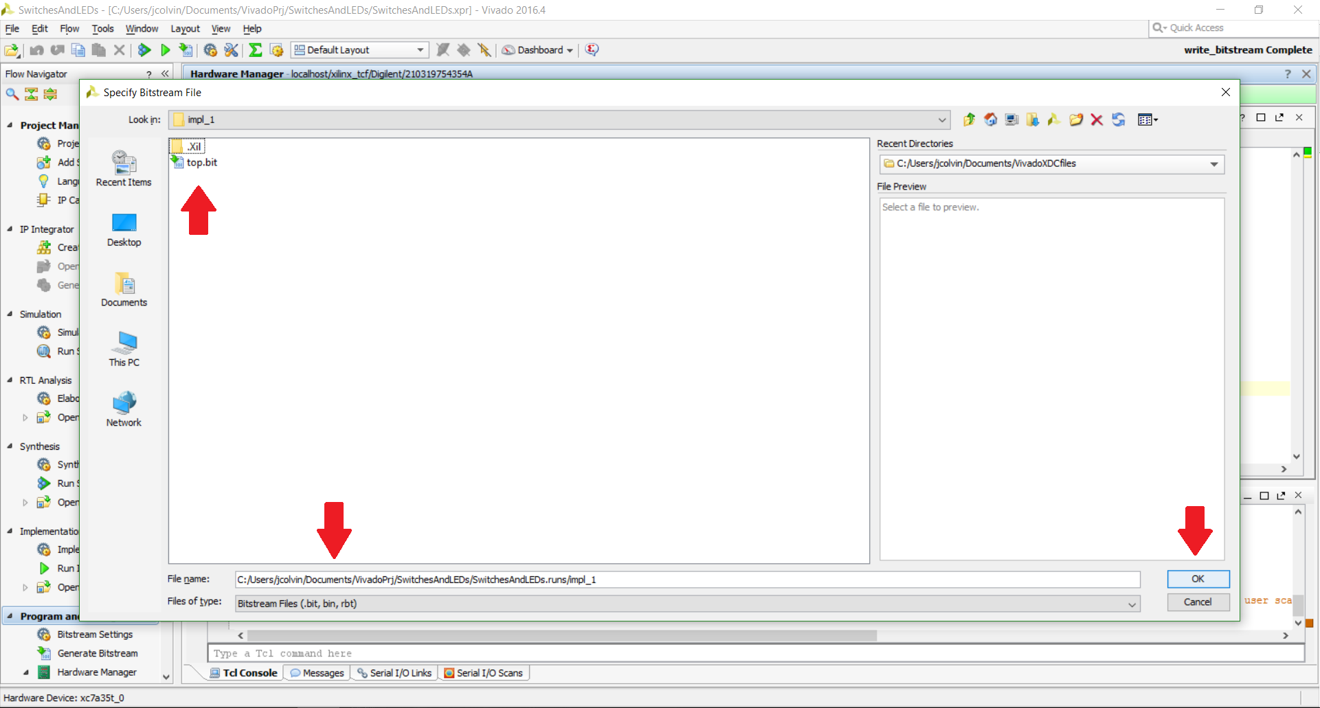
click program; this takes under 10 seconds for any computer, so it's not too bad.

Now we're done! The way this project was setup, the first switch (labeled SW0 on the Arty) controls the status of the first LED (labeled LD4 on the Arty).
need to make this look pretty rather than crazy with the picture labels and orientation. Perhaps I should do the whole picture captions beneath the image and the steps 1.1) with the arrows >… bother 
Multiple Switches and LEDs
The above assign statement gives the current value of sw (switch) to led (an LED). Because HDL in general (not just Verilog) describes an actual circuit that will be implemented onto the FPGA, rather than telling a processor what to do like in a microcontroller which is limited by its internal clock that dictates the timing the above statement that assigns the value of sw to led will essentially happen in real time, or at least as fast as it takes the electricity to propgate from the switch to the FPGA and then directly to the LED.
Important Takeaways from Project 2
tags to be added after I remove the spaces in the code below
learn programmable-logic software tutorial vivado verilog

