Genesys 2
- Programmable over JTAG and Quad-SPI Flash
- On-chip analog-to-digital converter (XADC)
(4 6-input LUTs & 8 flip-flops each)
and USB MSD host for storage
HPC connector w/ ten GTX lanes
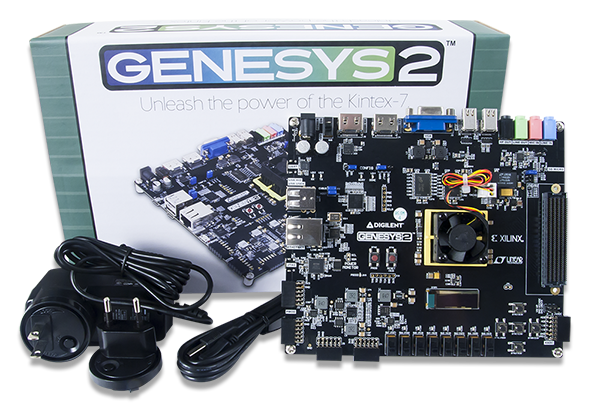
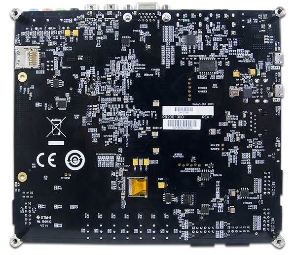
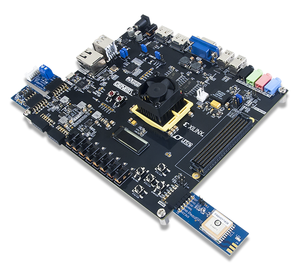
The Digilent Genesys 2 board is an advanced, high-performance, ready-to-use digital circuit development platform based on the latest Kintex-7™ Field Programmable Gate Array (FPGA) from Xilinx. With its high-capacity, high-speed FPGA (Xilinx part number XC7K325T-2FFG900C), fast external memories, high-speed digital video ports, and wide expansions options make the Genesys 2 well suited for data and video processing applications. Several built-in peripherals, including Ethernet, audio and USB 2.0, allow a wide range of other applications. The fully-bonded1) high-speed FMC HPC connector opens the door to great expansion possibilities.
Documentation
Note: Xilinx software tools are not available for download in some countries. Prior to purchasing the Genesys 2, please check the supporting software's availability, as it is required for the board's use.
Tutorials
- Genesys 2 - Getting Started with Microblaze Servers
- Genesys 2 - Programming Guide
- Getting Started with Digilent Pmod IPs
- Getting Started with Vivado
- Getting Started with Vivado IP Integrator and Xilinx SDK
- Installing Vivado, Xilinx SDK, and Digilent Board Files
Example Projects
Note: These example projects are supported in Vivado and Xilinx SDK 2016.4. No further updates are planned.


