Getting Started with Digilent Pmod IPs
Overview
Digilent Pmod IPs are only supported in Vivado and Xilinx SDK versions 2019.1 and earlier.
Digilent provides several IPs that are designed to make implementing and using a Pmod on an FPGA as straightforward as possible. This guide will describe how to use a Pmod IP core in Vivado Microblaze or Zynq design.
At the end of this tutorial you will have a Vivado design and demo for your FPGA or Zynq platform that uses a Digilent Pmod IP core.
The following two dropdown tables show which Digilent FPGA system boards and Pmods are supported by this tutorial, as well as some details about each one that you will need to know to complete this tutorial.
- Platforms Supported
- Pmods Supported
-
Pmod Interface Type Reference clock frequency (MHz) Reference Clock signal name Interrupt pin name/s Uses PmodGPIO Additional Notes 8LD GPIO - - - Yes - ACL SPI 80 ext_spi_clk - - - ACL2 SPI 50 ext_spi_clk - - - AD1 SPI - - - - - AD2 IIC - - - - - AD5 SPI 50 - - - - ALS SPI 50 ext_spi_clk - - - AMP2 GPIO - - timer_interrupt - - AQS IIC - - - - - BB GPIO - - - Yes - BLE UART - - - - - BT2 UART - - - - - BTN GPIO - - - Yes - CAN SPI 100 ext_spi_clk SPI_interrupt GPIO_interrupt - CLS SPI 50 ext_spi_clk - - - CMPS2 IIC - - - - SDK project requires math library COLOR IIC - - - - - DA1 SPI 50 ext_spi_clk - - - DHB1 PWM/GPIO - - - - - DPG1 SPI 50 ext_spi_clk - - - ENC GPIO - - - - - ESP32 UART - - - - - GPS UART - - gps_uart_interrupt - - GYRO SPI 50 ext_spi_clk - - - HYGRO IIC - - - - - JSTK SPI 16 ext_spi_clk - - - JSTK2 SPI 16 ext_spi_clk - - - KYPD GPIO - - - - - LED GPIO - - - Yes - MAXSONAR GPIO - - - - - MicroSD Use the Pmod SD IP core - MTDS SPI - - - - - NAV SPI/GPIO 50 ext_spi_clk - - - OLED SPI/GPIO - - - - - OLEDrgb SPI/GPIO 50 ext_spi_clk - - - PIR GPIO - - - - - R2R GPIO - - - - - RTCC IIC - - - - - SD SPI - - - - - SF3 SPI 50 ext_spi_clk QSPI_INTERRUPT - - SSR GPIO - - - Yes - SWT GPIO - - - Yes - TC1 SPI 50 ext_spi_clk - - TMP3 IIC - - - - WIFI SPI - - WF_INTERRUPT - Need 385 KB of BRAM or DDR
Prerequisites
Hardware
- Supported Digilent 7-Series FPGA System Board
- MicroUSB Cable/s
- One or More Supported Digilent Pmods
Software
- Xilinx Vivado 2018.2 with Xilinx SDK and Digilent Board Files
- Other versions of Vivado may work, but functionality is not guaranteed
- See the "Installing Vivado and Digilent Board Files" tutorial for more information.
- Digilent Vivado IP Library
- Step 2 of this tutorial covers how to download and extract these files.
Important
If the Pmod IP to be used has a README file, be sure to review it before starting this tutorial. This file can be found in the vivado-library/ip/Pmods/“your pmod” directory.
Tutorial
1. Create a New Microblaze/Zynq Block Design
To determine whether you need to use Microblaze or Zynq for this tutorial, refer to the entry in the Platforms Supported dropdown table found in the Overview Section of this tutorial. Alternatively, navigate to the resource center for your platform here.
- Microblaze
-
Follow the Getting Started with Vivado IP Integrator tutorial to obtain a basic MicroBlaze block design.
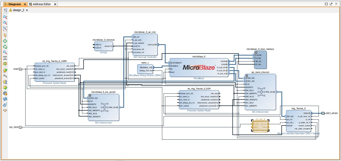
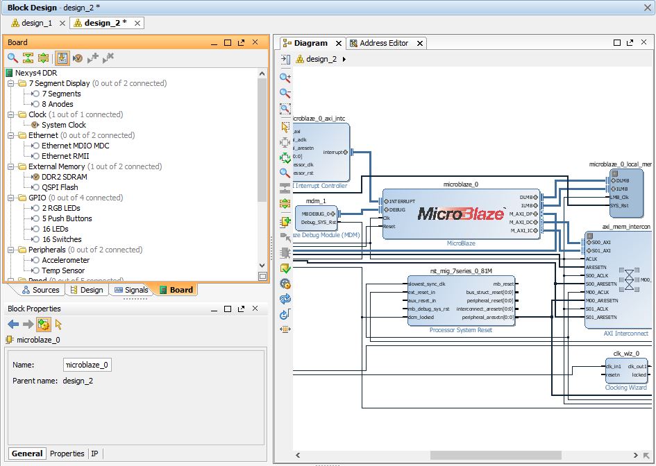
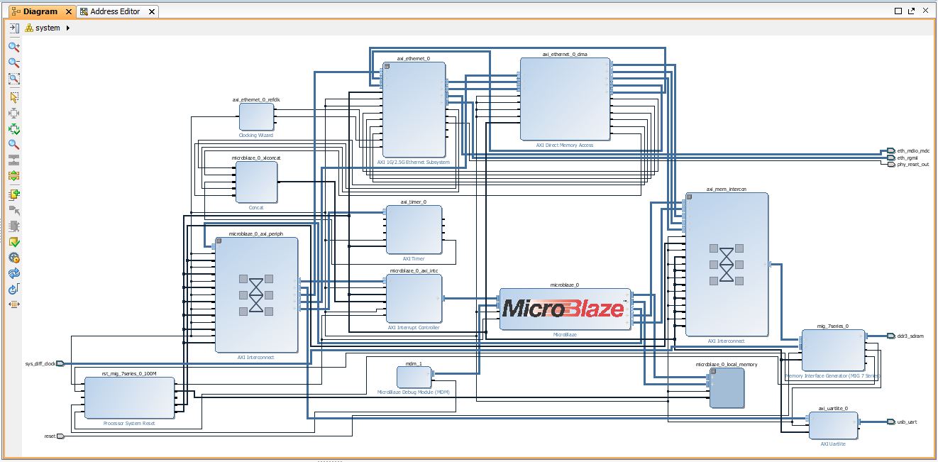
An example of a MicroBlaze block design for a board that has external DDR memory.
- Zynq
-
Follow the Getting Started with Vivado IP Integrator tutorial to obtain a basic Zynq block design.

An example of a Zynq block design.
2. Add the Digilent Library Repository
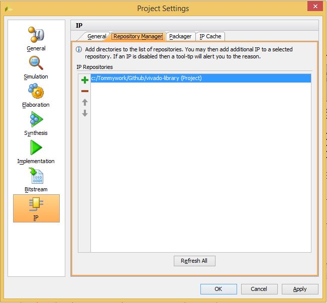
2.1) Find the latest release of Digilent's vivado-library repository where the version number matches the version of Vivado being used (example: “v2016.4-1” is the first release for Vivado 2016.4). Download the vivado-library-<version>.zip file (NOT one of the source code archives!), then extract this archive in a memorable location. This GitHub repository contains a large number of IP cores intended for use with Digilent boards, including all of Digilent's Pmod IP cores and Pmod interface description.
3. Add the Pmod to Your Block Design
Info
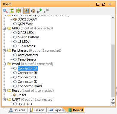
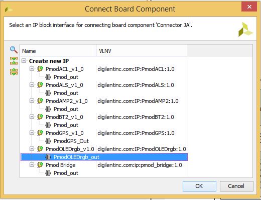
This list contains all of the components defined in the board file for your platform. You can use it to easily insert an IP block that will work with a piece of hardware found on your platform, for example an Ethernet port or general purpose LED. Several of these should have already been selected when you created your initial design in step 1.1.
Tip
Several of the simpler GPIO Pmods can be used with the PmodGPIO IP Core. To see if your Pmod is supported with this IP core consult the Pmod compatibility table found in the Overview Section of this tutorial.
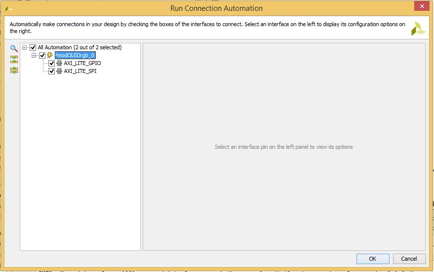
4. Run Connection Automation
5. Connect Reference Clocks
Important
Some Pmod IP cores require a reference clock to function properly. To see if your Pmod requires a reference clock consult the Pmod compatibility table found in the Overview Section. If your Pmod does not require a reference clock then skip to Step 6.
Attaching a reference clock to the Pmod IP core is different depending on which platform you are using. Select the tab that describes your platform best (consult the platform compatibility table in the Overview Section if you don't know).
- Zynq
-
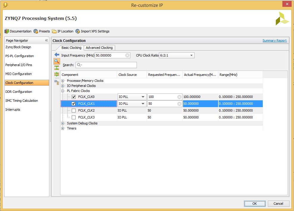
5.1) Double click the ZYNQ Processing System block to re-customize it. In the menu to the left, click Clock Configuration. Expand the PL Fabric Clocks drop down and check the first FCLK_CLK that is not already checked to activate it. Set the requested frequency to the frequency required for your Pmod. This frequency can be found in the Pmod compatibility chart in the Overview Section of this tutorial. Click OK.
Tip
If one of the FCLK_CLK's that is already checked has a frequency that matches the frequency needed for your pmod, you may use that clock. It is possible to connect a single clock to multiple destinations.
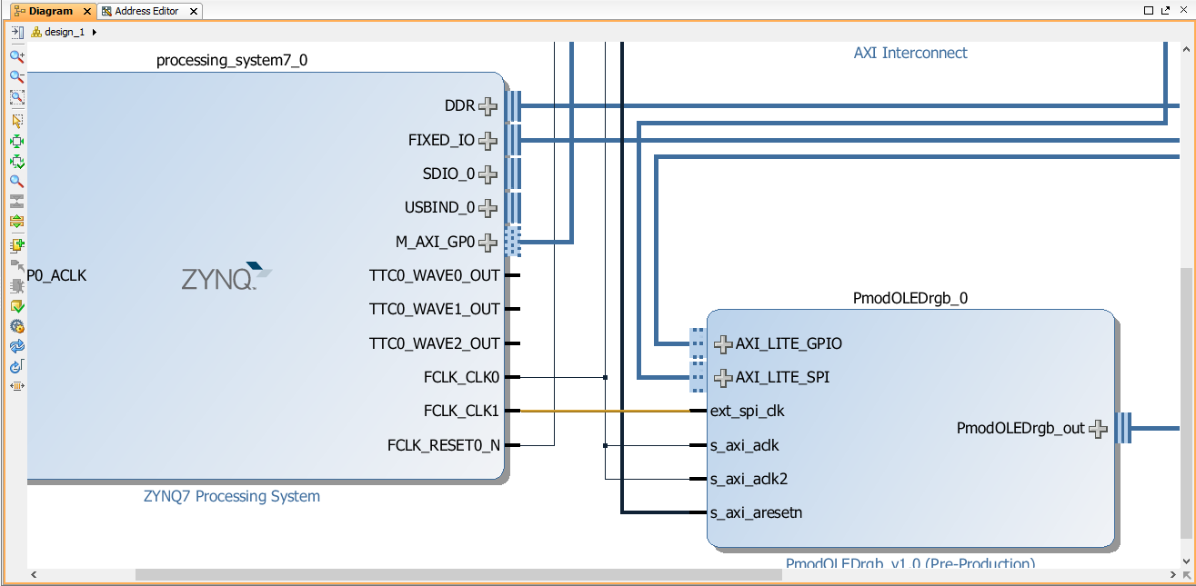
5.2) Connect this new clock to the clock input on your Pmod IP Core. The name of the clock input for your Pmod IP core can be found in the Pmod compatibility chart in the Overview Section of this tutorial.
- MicroBlaze with MIG
-
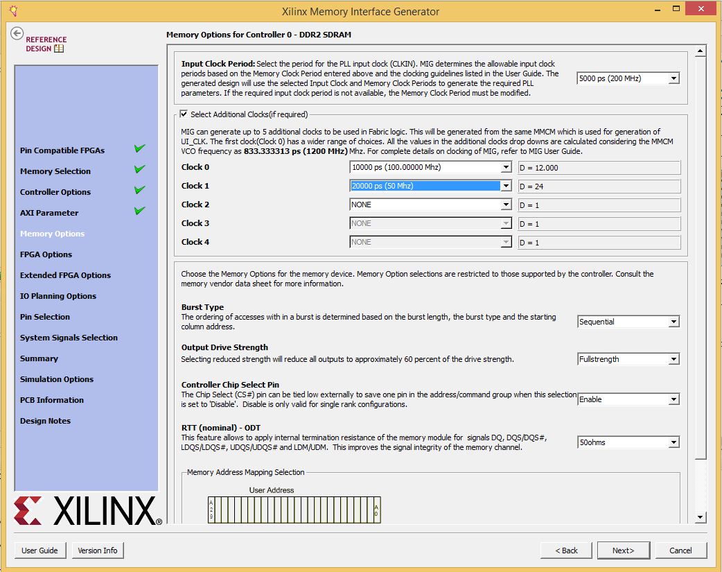
5.1) Double click the mig_7series block to re-customize it. In the Xilinx Memory Interface Generator window, keep clicking Next until you see Select Additional Clocks (shown below). Click this box and select the frequency required for your Pmod or the closest available slower frequency. The required frequency can be found in the Pmod compatibility chart in the Overview Section of this tutorial.
Tip
If one of the other clocks is already being used and has a frequency that matches the frequency needed for your Pmod then you may use that clock. It is possible to connect a single clock to multiple destinations. If this is the case, you may Cancel out of the MIG configuration dialog.
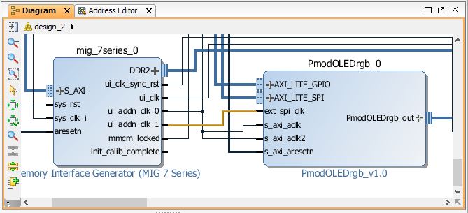
5.2) Keep clicking Next. When you reach the pin selection screen, click Validate and then OK. Keep clicking Next. Click Accept on the license agreement screen, then continue to click Next. Once you've reached the end, click Generate to regenerate your MIG block with your additional clocks.5.3) Connect this new clock to the clock input on your Pmod IP Core. The name of the clock input port for your Pmod IP core can be found in the Pmod compatibility chart in the Overview Section of this tutorial.
- MicroBlaze without MIG
-
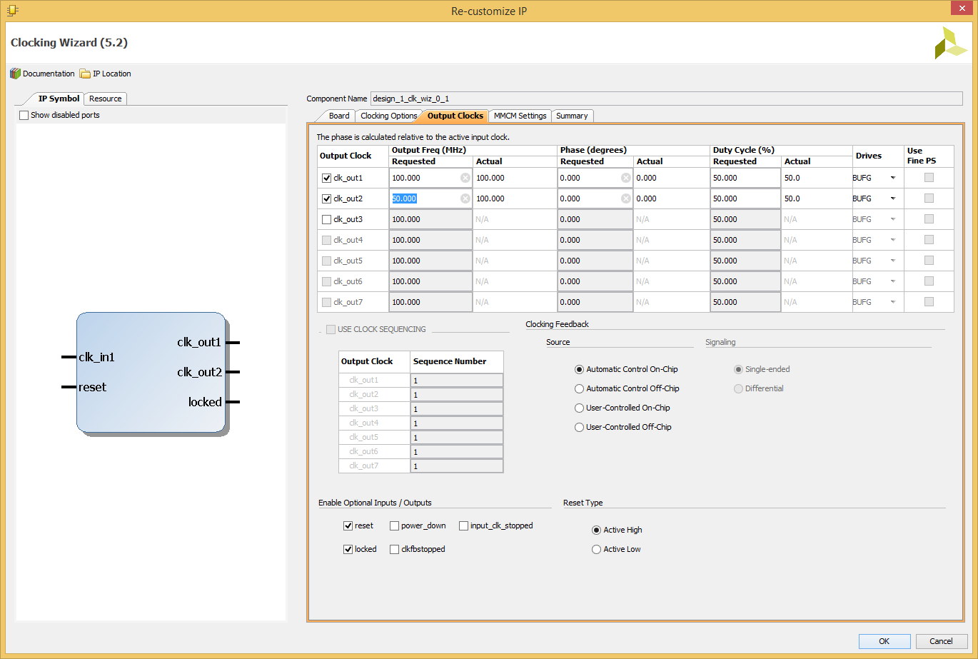
5.1) Double click the clocking wizard IP block to re-customize it. In the customization dialog, select the Output Clocks tab. Check the next clock that is not already checked to activate it. Set the requested output frequency to the frequency required for your Pmod. This frequency can be found in the Pmod compatibility chart in the Overview Section of this tutorial. Click OK.
Tip
If one of the other clocks is already being used and has a frequency that matches the frequency needed for your Pmod then you may use that clock. It is possible to connect a single clock to multiple destinations.
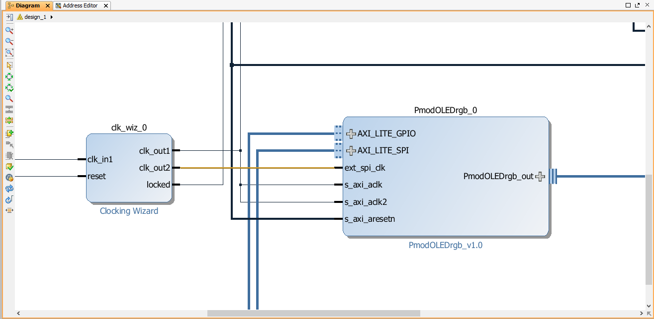
5.2) Connect this new clock to the clock input on your Pmod IP Core. The name of the clock input for your Pmod IP core can be found in the Pmod compatibility chart in the Overview Section of this tutorial.
6. Connect Interrupts
Important
Some Pmod IP cores require an interrupt to function properly. To see if your Pmod requires an interrupt consult the Pmod compatibility table found in the Overview Section. If your Pmod does not require an interrupt then skip to Step 7.
Attaching a Pmod IP core interrupt to the processor is different depending on which platform you are using. Select the tab that describes your platform best (consult the platform compatibility table in the Overview Section if you don't know).
- Zynq
-
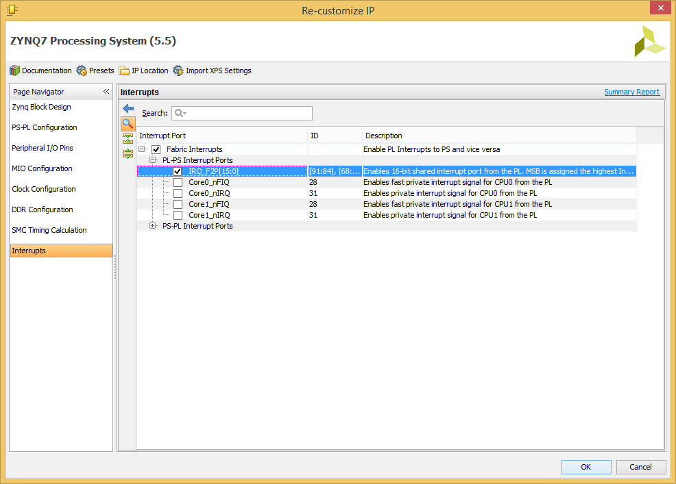
6.2) Add a Concat IP core to the block design. Re-customize the concat block to make sure that the number of inputs matches the number of interrupts you need to connect to your Zynq Processor - probably only one. Click Ok.
- Microblaze
-
6.1) If your MicroBlaze block doesn't have an AXI Interrupt Controller connected to it's INTERRUPT port, add an AXI Interrupt controller to your block design. Manually connect the interrupt port of the axi_intc_0 to the INTERRUPT port of your MicroBlaze block. Use Connection Automation to connect it's AXI interface to the rest of the system.
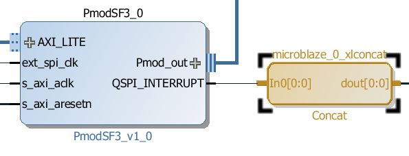
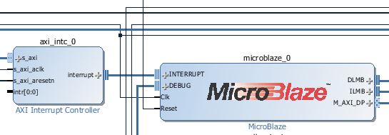 6.2) Add a Concat IP core to the block design. Re-customize the concat block to make sure that the number of inputs matches the number of interrupts you need to connect to your Microblaze Processor - probably only one. Click Ok.
7. Validate the Design
7.1) Click theRegenerate Layout button to rearrange your block design.
7.2) SelectValidate Design. This will check for design and connection errors.
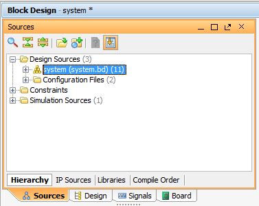
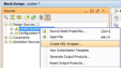
7.3) If you have already created an HDL wrapper for your block design as part of the board specific Getting Started With… tutorial, skip the remainder of this step. Otherwise, after the design validation step we will proceed with creating a HDL System Wrapper. Click on the Sources tab and find your block design.
7.4) Right click on your block design and click Create HDL Wrapper. Let Vivado manage the wrapper and automatically update it and click OK.
This will create a top module in VHDL and will allow you to generate a bitstream.
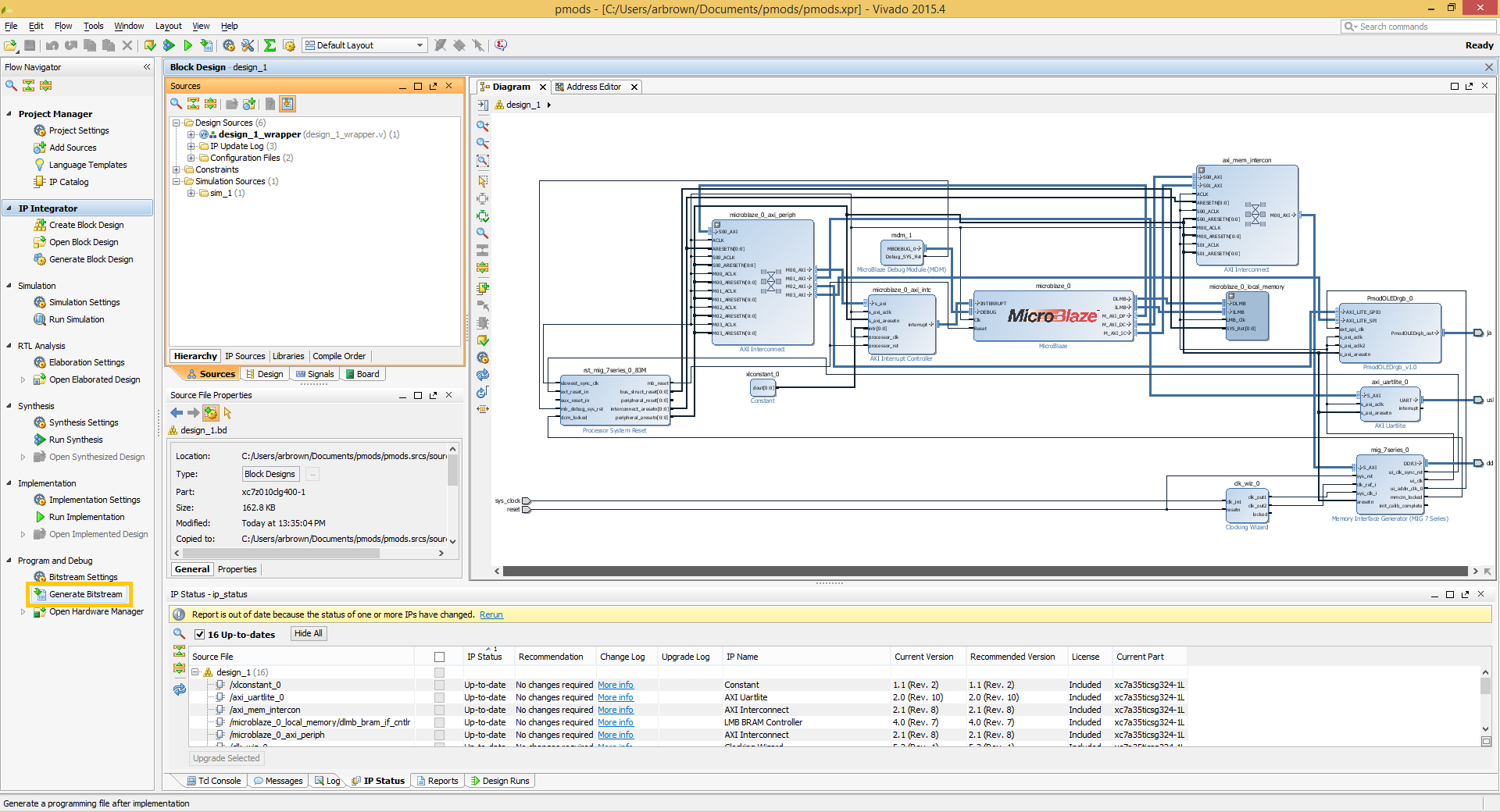
8. Generate the Bit File
8.2) The bit file generation will begin. The tool will run Synthesis and Implementation. After both have been successfully completed, the bit file will be created. You will find a status bar of Synthesis and Implementation running on the top right corner of the project window.
This process can take anywhere from 5 to 60 minutes depending on the computer Vivado is running on and the size of the target FPGA.
8.3) After the bitstream has been generated, a message prompt will pop-up on the screen. You don't have to open the Implemented Design for this demo. Just click Cancel.
9. Export the Hardware Design to SDK
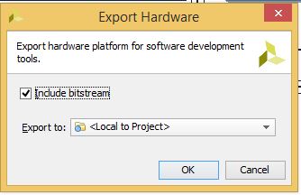
9.1) At the top of the Vivado window, click File → Export → Export Hardware. Check the box to Include Bitstream and click OK. This will give Xilinx SDK all of the information it needs to know about the hardware design, as well as the files needed to program the hardware onto a target FPGA system board.
A new file directory will be created in the project directory under echo_server.SDK similar to the Vivado hardware design project name. Two other files, .sysdef and .hdf are also created. This step essentially creates a new SDK Workspace.
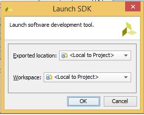
9.2) On the main toolbar, click File → Launch SDK. Leave both of the dropdown menus as their default <Local to Project> and click OK. This will open Xilinx SDK and import the exported hardware.
10. Xilinx SDK
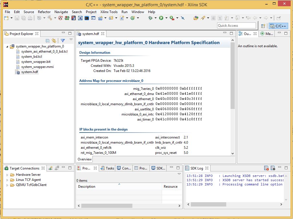
The HW design specification and included IP blocks are displayed in the “system.hdf” file. Xilinx SDK is independent of Vivado, i.e. from this point, you can create your SW project in C/C++ on top of the exported HW design. If necessary, SDK can be launched directly with the <PROJECT>.sdk folder in the main Vivado project directory as the workspace. From this point, if you need to go back to Vivado and make changes to the HW design, then it is recommended to close the SDK window and make the required HW design edits in Vivado. After this you must follow the sequence of saving design, allowing Vivado to regenerate the HDL wrapper, and generating a new bit file. This new bit file and modified hardware design must then be exported to SDK.
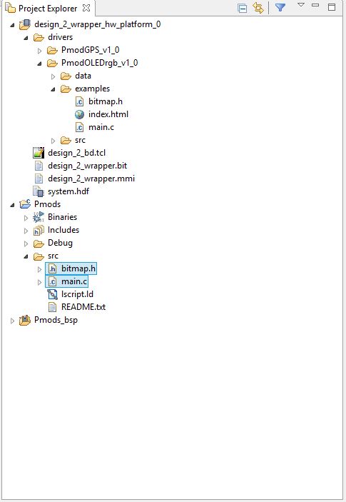
Within the Project Explorer tab on the left, you can see the hardware platform project. The name of the hardware platform follows the name of the block design wrapper created in Vivado. This hardware platform has all the HW design definitions, IP interfaces that have been added, external output signal information and local memory address information.
The drivers for any Pmod IPs in the design can be found in the appropriate folder in the hardware platform, under /drivers. If you want to edit these drivers, use the versions found in the board support package project under libsrc/. If you do modify the drivers, keep in mind that any changes to your hardware will overwrite these changes, as well as any use of the Regenerate BSP Sources option.
11. Create a New Application Project in SDK
You will see two new folders in the Project Explorer panel.
- Your application project which contains all the binaries, .C and .H (Header) files
- The board support package for your project, which contains driver source files that your project may include
Our main working source folder also contains an important file shown here which is the “lscript.ld”. This is a Xilinx auto generated linker script file and includes information about memory addresses for different IP components of your block design, as well as the sizes of other memory regions.
12. Import the Example Project
13. Program the FPGA with the Bit File
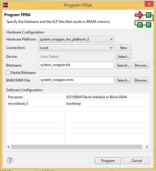
13.1) Make sure that your board is turned on and connected to the host PC with micro USB cables for UART and programming. On some boards, you will only need to connect a single PROG/UART port while on others you will need to connect your PC to two different ports typically named UART and PROG or JTAG. On the top toolbar, click theProgram FPGA button. Some boards will also require that they be connected to a separate power source.
13.2) Click Program to program your FPGA with your hardware design.
14. Program the Microblaze/ZYNQ Processor
14.1) The majority of demos require that you use a serial terminal on your PC to read messages printed by the demo. Settings for the terminal will vary depending on your board, but typically you will need to use a baud rate of 115200 or 9600, 8 bit data, no parity bit, and one stop bit. Zynq projects will use 115200 baud, while the baud rate for MicroBlaze projects will depend on the configuration of the Uartlite IP in Vivado.
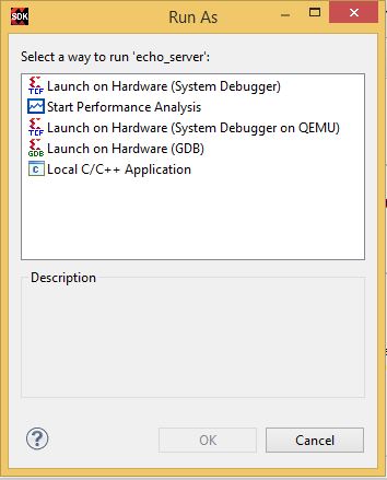
14.2) Select your application project and click theRun As… button. Select Launch on Hardware (System Debugger) and click OK.
14.3) Xilinx SDK will run the program starting in main.c on your Microblaze/Zynq processor. Review the comment header at the top of the example main file to get more information on what the demo does, as well as any additional setup requirements.

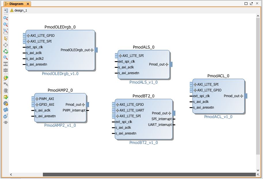
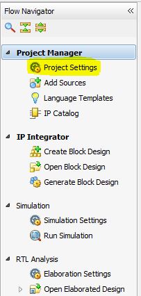


 Generate Bitstream. This can also be found in the Flow Navigator panel on the left, under Program and Debug. If you haven't already saved your design, you will get a prompt to save the block design.
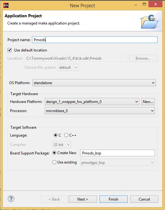
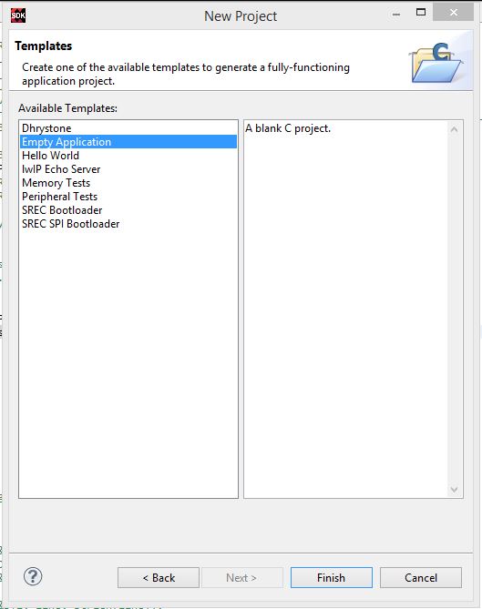
 New dropdown arrow and select Application Project.