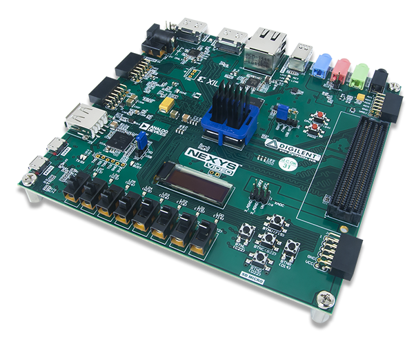
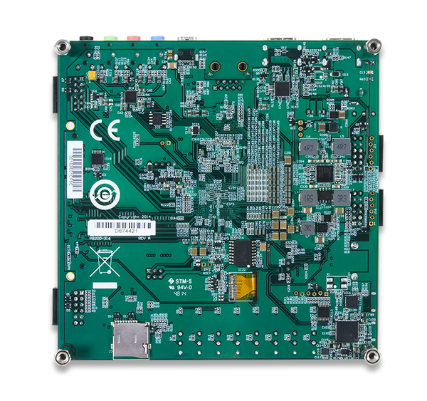
Nexys Video Reference Manual
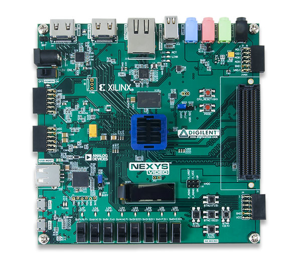
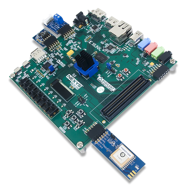
The Nexys Video board is a complete, ready-to-use digital circuit development platform based on the latest Artix-7™ Field Programmable Gate Array (FPGA) from Xilinx®. With its large, high-capacity FPGA (Xilinx part number XC7A200T-1SBG484C), generous external memories, high-speed digital video ports, and 24-bit audio codec, the Nexys Video is perfectly suited for audio and video processing applications. Several built-in peripherals, including Ethernet, USB-UART, and a high bandwidth USB data transfer protocol, expand the connectivity of the Nexys Video so that it can be cleanly integrated as a single component of a large system. The Nexys Video also includes provisions for direct human interaction with a connector for USB-HID devices, an OLED Display, and a vast assortment of switches, buttons, and LEDs. Lastly, the FMC and Pmod ports can be used to add virtually any functionality or connection interface your application demands.
Download This Reference Manual
Features
- 33,650 logic slices, each with four 6-input LUTs and 8 flip-flops
- Close to 13 Mbits of fast block RAM (3x more than the Nexys 4 DDR)
- Ten clock management tiles, each with phase-locked loop (PLL)
- 740 DSP slices
- Internal clock speeds exceeding 450 MHz
- On-chip analog-to-digital converter (XADC)
- Up to 3.75Gbps GTP transceivers
- 8 user switches
- USB-UART Bridge
- HDMI Sink and HDMI Source
- 6 user push buttons
- 512MiB 800MT/s DDR3
- Pmod for XADC signals
- 8 user LEDs
- 160-pin FMC LPC connector
- DisplayPort Source
- User EEPROM
- Serial Flash
- Digilent Adept USB port for programming and data
- 128×32 monochrome OLED display
- MicroSD card connector
- Audio codec w/ four 3.5mm jacks
- 10/100/1000 Ethernet PHY
- Four Pmod ports
- USB HID Host for mice, keyboards and USB MSD Host
In addition to being compatible with Xilinx's ISE® toolset, the Nexys Video also works with the new high-performance Vivado ® Design Suite. It is supported under the free WebPACK™ license, so designs can be implemented at no additional cost. This free license now includes the ability to create MicroBlaze™ soft-core processor designs (in Vivado only), which greatly reduces the time needed to implement complex systems.
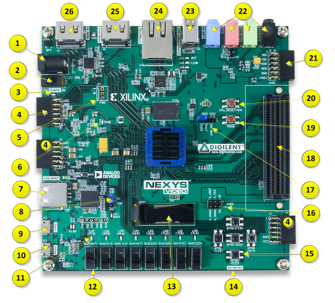
| Callout | Component Description | Callout | Component Description |
|---|---|---|---|
| 1 | Power jack | 14 | MicroSD card slot (underneath) |
| 2 | Power Switch | 15 | Five pushbuttons |
| 3 | Power indicator LED | 16 | Miscellaneous XADC pins |
| 4 | Pmod Header(s) | 17 | Programming mode jumper |
| 5 | External fan control solder points | 18 | FMC header |
| 6 | FPGA programming done LED | 19 | FPGA configuration reset button |
| 7 | USB host connector | 20 | CPU reset button (for soft cores) |
| 8 | External configuration jumper (SD / USB) | 21 | Analog signal Pmod header (JXADC) |
| 9 | Micro USB (UART) connector | 22 | Microphone/Audio connectors |
| 10 | Micro USB (JTAG) connector for USB programming | 23 | DisplayPort output connector |
| 11 | LEDs (8) | 24 | Ethernet connector |
| 12 | Slide Switches (8) | 25 | HDMI output connector |
| 13 | OLED display | 26 | HDMI input connector |
Regulatory warnings
Warning This is a class A product. In a domestic environment this product may cause radio interference in which case the user may be required to take adequate measures.
1. Power Supplies
The Nexys Video board can receive power from an external power supply through the center-positive barrel jack (J21) or the two-pin battery header (J22). The external supply voltage must be 12 V ±5 %. The Nexys Video cannot be powered from the USB bus.
All Nexys Video power supplies can be turned on and off by a single logic-level power switch (SW8). Enables of power supplies not connected directly to the power switch are disabled indirectly. A power-good LED (LD16), driven by the “power good” output of the on-board regulators, indicates that the supplies are turned on and operating normally. An overview of the Nexys Video power circuit is shown in Fig. 1.
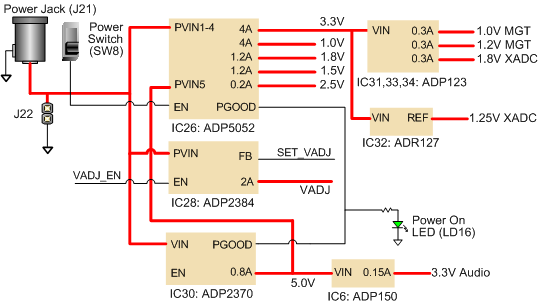 Figure 1. Nexys Video power circuit.
An external power supply can be used by plugging it into the power jack (J21). The supply must use a coax, center-positive 2.1mm internal-diameter plug, and deliver 12VDC ±5 %. The minimum current rating of the supply depends on the actual design implemented in the FPGA, but at least 3A of current (i.e., at least 36W of power) is recommended.
Instead of a wall supply, an external battery pack can be used by connecting the battery’s positive terminal to the positive pin of J22 and the negative terminal to the negative pin. Incorrect polarity might cause permanent damage to the board. To power the Nexys Video and any peripheral other than an FMC mezzanine card using the 12P0V supply, the battery voltage must be in the 6-15 V range. Since the external power supply pin is wired directly to the 12P0V pin of the FMC connector, the battery voltage must be 12VDC ±5 % in FMC applications, the same as the wall supply specification. In any case, 15V is an absolute maximum.
Voltage regulator circuits from Analog Devices® create the different voltages required by the FPGA and on-board peripherals from the main power input. Some regulators use the outputs of another regulator as input, depending on design considerations. In some cases this chaining helps in creating the proper power-on sequence for circuits. In other cases the chaining of power supply enables achieves the same purpose.
Table 1 provides information on maximum and typical currents for each power rail. The typical currents strongly depend on FPGA configuration and the values provided are typical of medium size/speed designs.
| Supply | Circuits | Device | Current (max/typical) |
|---|---|---|---|
| 3.3 V | FPGA I/O, USB, FMC, Clocks, Pmod, Ethernet, SD slot, Flash, DisplayPort | IC26: ADP5052 | 4A / 0.1 to 1.5A |
| 1.0 V | FPGA Core | IC26: ADP5052 | 4A / 0.2 to 2A |
| 1.8 V | FPGA Auxiliary | IC26: ADP5052 | 1.2A / 0.15A |
| 1.5 V | DDR3 and FPGA I/O | IC26: ADP5052 | 1.2 A / 0.5 A |
| 2.5 V | FPGA I/O and Ethernet | IC26: ADP5052 | 0.2 A / 0.1 A |
| VADJ (1.2-3.3 V) | User I/O, FMC, and FPGA I/O | IC28: ADP2384 | 2 A / 0.1 A |
| 3.3 V | Audio analog supply | IC6: ADP150 | 0.15 A / 0.05 A |
| 5.0 V | USB Host, HDMI | IC30: ADP2370 | 0.8 A / 0.5 A |
| MGT 1.0 V | Gigabit Transceivers VCC | IC31: ADP123 | 0.3 A |
| MGT 1.2 V | Gigabit Transceivers VTT | IC33: ADP123 | 0.3 A |
| XADC 1.8 V | XADC supply | IC34: ADP123 | 0.3 A |
| XADC 1.25 V | XADC reference | IC32: ADR127 | 5 mA |
Table 1. Voltage rail power ratings
The VADJ power rail requires special attention. It is a programmable voltage rail that power the FMC mezzanine connector, user push-buttons, switches, XADC Pmod connector, and the FPGA banks connected to these peripherals (banks 15, 16). The feedback pin of the VADJ regulator is connected to an analog multiplexer controlled by two FPGA signals, “SET_VADJ(1:0)”. The multiplexer is able to change the resistor values in the feedback loop, thereby changing the voltage on the regulator’s output. Depending on the value set on the “SET_VADJ(1:0)” pins, the possible voltages are listed in Table 2. The third control pin is the “VADJ_EN” signal, which can disable the regulator altogether. If these control pins are not used in the FPGA design, on-board pull resistors enable the regulator and set the VADJ voltage to 1.2 V.
An FPGA design can dynamically change the VADJ voltage to suit a certain FMC mezzanine card or application. Care must be taken to disable the regulator first by bringing “VADJ_EN” low, setting “SET_VADJ(1:0)” and enabling the regulator again. Please note that for proper voltage levels in digital signals connected to VADJ-powered FPGA banks (ex. user push-buttons), the correct I/O standard still needs to be set in the design user constraints (XDC or UCF file). See the schematic and/or the constraints file to determine which signals are in VADJ-powered banks. The provided master UCF and XDC files assume the default VADJ voltage of 1.2V, declaring LVCMOS12 as the I/O standard for these signals.
| SET_VADJ(1:0) | VADJ |
|---|---|
| 00 (default) | 1.2 V |
| 01 | 1.8 V |
| 10 | 2.5 V |
| 11 | 3.3 V |
Table 2. VADJ programmable voltages
2. FPGA Configuration
After power-on, the Artix-7 FPGA must be configured (or programmed) before it can perform any functions. You can configure the FPGA in one of four ways:
- A PC can use the Digilent USB-JTAG circuitry (port J12, labeled “PROG”) to program the FPGA any time the power is on.
- A file stored in the non-volatile serial (SPI) flash device can be transferred to the FPGA.
- A programming file can be transferred to the FPGA from a microSD card.
- A programming file can be transferred from a USB mass-storage device (ex. pen drive) attached to the USB HID port.
Figure 3 shows the different options available for configuring the FPGA. An on-board “mode” jumper (JP4) and a media selection jumper (JP3) select between the programming modes.
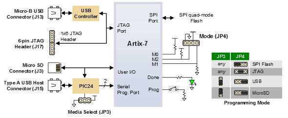 Figure 2. Nexys Video configuration options
The FPGA configuration data is stored in files called bitstreams that have the .bit file extension. The ISE or Vivado software from Xilinx can create bitstreams from VHDL or Verilog. In Vivado, the IP Integrator tool can also be used, which provides a graphical, block diagram-based design environment.
Bitstreams are stored in volatile memory cells within the FPGA. This data defines the FPGA's logic functions and circuit connections, and it remains valid until it is erased by removing board power, by pressing the reset button attached to the PROG input, or by writing a new configuration file using the JTAG port.
An Artix-7 200T bitstream is typically 77,845,216 bits and can take a long time to transfer depending on the programming mode. The time it takes to program the Nexys Video can be decreased by compressing the bitstream before programming, and then allowing the FPGA to decompress the bitstream itself during configuration. Depending on design complexity, compression ratios of 10x can be achieved. Bitstream compression can be enabled within the Xilinx tools (ISE or Vivado) to occur during generation. For instructions on how to do this, consult the Xilinx documentation for the toolset being used. This option is available for all programming modes.
Mode-specific speed-ups are also available. JTAG clock frequency can be set to the maximum supported by the programming cable in iMPACT/Vivado Hardware Manager. Similarly, the clock frequency for the SPI Flash can be increased in device properties (Vivado) or bitstream generation options (ISE). The microSD and USB mass-storage device configuration modes already operate at their maximum possible speed.
After being successfully programmed, the FPGA will cause the “DONE” LED to illuminate. Pressing the “PROG” button at any time will reset the configuration memory in the FPGA. After being reset, the FPGA will immediately attempt to reprogram itself from whatever method has been selected by the programming mode jumpers.
The following sections provide greater detail about programming the Nexys Video using the different methods available.
2.1. JTAG Programming
The Xilinx tools typically communicate with FPGAs using the Test Access Port and Boundary-Scan Architecture, commonly referred to as JTAG. During JTAG programming, a .bit file is transferred from the PC to the FPGA using the onboard Digilent USB-JTAG circuitry (port J12) or an external JTAG programmer, such as the Digilent JTAG HS2, attached to port J17. You can perform JTAG programming at any time after the Nexys Video has been powered on, regardless of what the mode jumper (JP4) is set to. If the FPGA is already configured, then the existing configuration is overwritten with the bitstream being transmitted over JTAG. Setting the mode jumper to the JTAG setting is useful to prevent the FPGA from being configured from any other bitstream source until a JTAG programming occurs.
Programming the Nexys Video with an uncompressed bitstream using the on-board USB-JTAG circuitry usually takes around four seconds with a 30 MHz JTAG clock.
JTAG programming can be done using the hardware server in Vivado or the iMPACT tool included with ISE. The Nexys Video Programming Guide available on the Nexys Video Resource Center walks through the process of building a bitstream and using it to program the Nexys Video.
2.2. Quad-SPI Programming
For the FPGA to be able to configure itself from the SPI Flash, it first needs to be programmed with the bitstream. This is called indirect programming and is a two-step process controlled by Hardware Manager (Vivado) or iMPACT (ISE). First, the FPGA is programmed with a design that can program flash devices, and then data is transferred to the flash device via the FPGA circuit (this complexity is hidden from the user by the Xilinx tools). After the flash device has been programmed, it can automatically configure the FPGA at a subsequent power-on or reset event as determined by the mode jumper setting. Programming files stored in the flash device will remain until they are overwritten, regardless of power-cycle events.
Programming the flash can take as long as four to five minutes, which is mostly due to the lengthy erase process inherent to the memory technology. Once written however, FPGA configuration can be very fast; taking less than a second. Bitstream compression, SPI bus width, and configuration rate are factors controlled by the Xilinx tools that can affect configuration speed. The on-board flash has a Quad-SPI interface, which supports single (x1), dual (x2), and quad (x4) modes. The quad mode results in the fastest possible data transfer rate. For it to work, the bitstream needs to be generated with the x4 bus width option (Vivado device property) and the nonvolatile quad configuration bit in the flash to be enabled. The Nexys Video is shipped with this bit enabled.
Indirect programming of the flash can also be done using the iMPACT tool included with ISE. The correct part to be set in the tools is s25fl256xxxxxx0 from the manufacturer Spansion®.
The Nexys Video Programming Guide available on the Nexys Video Resource Center walks through the process of programming the Quad-SPI flash from Vivado.
2.3. USB Host and Micro SD Programming
You can program the FPGA from a pen drive attached to the USB-HID port (J15) or a microSD card inserted into J3 by doing the following:
- Format the storage device (pen drive or microSD card) with a FAT32 file system.
- Place a single .bit configuration file in the root directory of the storage device.
- Attach the storage device to the Nexys Video.
- Set the JP4 Programming Mode jumper on the Nexys Video to “USB/SD”.
- Select the desired storage device using JP3.
- Push the PROG button or power-cycle the Nexys Video.
The FPGA will automatically configure with the .bit file on the selected storage device. Any .bit files that are not built for the proper Artix-7 device will be rejected by the FPGA.
The Auxiliary Function Status, or “BUSY” LED (LD14), gives visual feedback on the state of the configuration process when the FPGA is not yet programmed:
- When steadily lit, the auxiliary microcontroller is either booting up or currently reading the configuration medium (microSD or pen drive) and downloading a bitstream to the FPGA.
- A slow pulse means the microcontroller is waiting for a configuration medium to be plugged in.
- In case of an error during configuration, the LED will blink rapidly. It could be that the device plugged in is not recognized, it is not properly formatted, or the bitstream is not compatible with the FPGA.
When the FPGA has been successfully configured, the behavior of the LED is application-specific. For example, if a USB keyboard is plugged in, a rapid short blink will signal the receipt of an HID input report from the keyboard.
3. Memory
The Nexys Video board contains two external memories: a 512MiByte volatile DDR3 memory and a 32MiByte non-volatile Serial Flash device. The DDR3 uses a 16-bit wide memory component soldered on the board with industry-standard interface. The Serial Flash is on a dedicated quad-mode (x4) SPI bus.
3.1. DDR3
The Nexys Video includes one DDR3 memory component creating a single rank, 16-bit wide interface. It is routed to a 1.5V-powered high range (HR) FPGA bank with 50 ohm controlled single-ended trace impedance. 50 ohm internal terminations in the FPGA are used to match the trace characteristics. Similarly, on the memory side on-die terminations (ODT) are used for impedance matching.
Note: The Nexys Video may use any of the Micron MT41K256M16HA-187E, Micron MT41K256M16TW-107, Zentel A3T4GF40ABF-GML, or Zentel A3T4GF40BBF-HP DDR3 parts. User projects targeting previous revisions of the board which only included the MT41K256M16HA-187E part will be backward-compatible with any of the loaded parts.
For proper operation of the memory, a memory controller and physical layer (PHY) interface needs to be included in the FPGA design. The Xilinx 7 series memory interface solutions core generated by the memory interface generator (MIG) Wizard hides away the complexities of a DDR3 interface. Depending on the tool used (ISE, EDK, or Vivado), the MIG Wizard can generate a native FIFO-style or an AXI4 interface to connect to user logic. This workflow allows the customization of several DDR3 parameters optimized for the particular application. Table 2 below lists the MIG Wizard settings optimized for the Nexys Video.
| Setting | Value |
|---|---|
| Memory type | DDR3 SDRAM |
| Max. clock period | 2500ps (800MT/s data rate) |
| Clock ratio | 4:1 |
| Memory type | Components |
| Memory part | MT41K256M16HA-125 |
| Memory voltage | 1.5V |
| Data width | 16 |
| Data mask | Enabled |
| Input clock period | 10000ps (100 MHz) |
| Output driver impedance | RZQ/6 |
| Chip Select pin | Disabled |
| Rtt (nominal) – On-die termination | RZQ/6 |
| Internal Vref | Enabled |
| Internal termination impedance | 50ohms |
Table 3. DDR3 settings for the Nexys Video.
The MIG Wizard will require the fixed pin-out of the memory signals to be entered and validated before generating the IP core. For your convenience an importable UCF file and MIG .prj file is provided on the Nexys Video Resource center to speed up the process.
For more details on the Xilinx memory interface solutions refer to the 7 Series FPGAs Memory Interface Solutions User Guide (ug586).
3.2. Quad-SPI Flash
Non-volatile storage is provided by a Spansion S25FL256S flash memory. FPGA configuration files can be written to it, and mode settings are available to cause the FPGA to automatically read a configuration from this device at power on. An Artix-7 200T configuration file requires just over 9 MiB (mebibyte) of memory, leaving about 70% of the flash device available for user data. Or, if the FPGA is getting configured from another source, the whole memory can be used for custom data.
The contents of the memory can be manipulated by issuing certain commands on the SPI bus. The implementation of this protocol is outside the scope of this document. All signals in the SPI bus, except SCK, are general-purpose user I/O pins after FPGA configuration. SCK is an exception because it remains a dedicated pin even after configuration. Access to this pin is provided through a special FPGA primitive called STARTUPE2.
NOTE: Refer to the manufacturer’s data sheets and Xilinx user guides for more information.
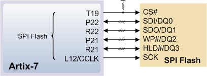
Figure 3. Nexys Video SPI Flash pinout.
4. Ethernet PHY
The Nexys Video board includes a Realtek RTL8211E-VL PHY paired with an RJ-45 Ethernet jack with integrated magnetics to implement a 10/100/1000 Ethernet port for network connection. The PHY interfaces with the FPGA via RGMII for data and MDIO for management. Bank 13 powered at 2.5V is populated with these signals. The auxiliary interrupt (INT_B) and power management (PME_B) signals are also wired to bank 13. The reset signal (RST_B) is the only one wired to a different bank (34), powered at 3.3V. The connection diagram can be seen in Fig. 4.
At power-on reset, the PHY is set to the following defaults using the configuration pins in parenthesis:
- Auto-negotiation enabled, advertising all 10/100/1000 modes (AN[1:0])
- PHY address=00001 (PHY_AD[2:0])
- No delay for TXD and RXD relative to TXC and RXC for data latching (RXDLY, TXDLY)
If an Ethernet cable is plugged in, establishing link is attempted straight after power-up, even if the FPGA is not programmed.
Three status indicator LEDs are on-board near the RJ-45 connector that indicate traffic (LD10) and valid link state (LD9). Table 4 below shows the default behavior.
| Function | Designator | State | Description |
|---|---|---|---|
| ACT | LD10 | Blinking | Transmitting or receiving |
| LINK | LD9 | On | Link up |
| Blinking 0.4s ON, 2s OFF | Link up, Energy Efficient Ethernet (EEE) mode | ||
| USER | LD8 | On | Link up, no traffic |
| Off | Link down | ||
| Blinking | Link up, traffic |
Table 4. Ethernet status LEDs
The on-board PHY implements Layer 1 in the Ethernet stack, interfacing between the physical copper medium and the media access control (MAC). The MAC must be implemented in the FPGA and mapped to the PHY's RGMII interface. Vivado-based designs can use the Xilinx AXI Ethernet Subsystem IP core to implement the MAC and wire it to the processor and the memory subsystem. At the time of writing, the IP core needed to be licensed separately with Xilinx part number EF-DI-TEMAC-PROJ or EF-DI-TEMAC-SITE. A free evaluation of this core is available, however, the design will stop working after running for approximately 8 hours.
The RGMII interface requires a data to clock skew of 1.0-2.6 ns at the receiver: at the FPGA for ETH_RX* and at the PHY for ETH_TX*. The PCB traces do not introduce the required skews. Consequently, either the PHY or the MAC IP in the FPGA has to introduce them. The PHY may be configured by moving resistors R88 to R83 (RXDLY) and R79 to R72 (TXDLY). This will have the effect of adding 2 ns.
On an Ethernet network each node needs a unique MAC address. To this end a Microchip 24AA025E48 EEPROM is provided on the Nexys Video. On one hand it is a read-writeable EEPROM that can be accessed via I2C. On the other hand it features a read-only memory section that comes pre-programmed with a unique identifier. This unique identifier can be read and used as a MAC address, avoiding a possible address conflict on the network. The device address and control code of the EEPROM is 1010111b. The out-of-box Ethernet demo uses the unique MAC to allow connecting several Nexys Video boards to the same network.
A tutorial that describes how to create a simple server using a MicroBlaze softcore processor and the Xilinx AXI Ethernet Subsystem IP core is available on the Nexys Video resource center.
Use only shielded Ethernet cables.
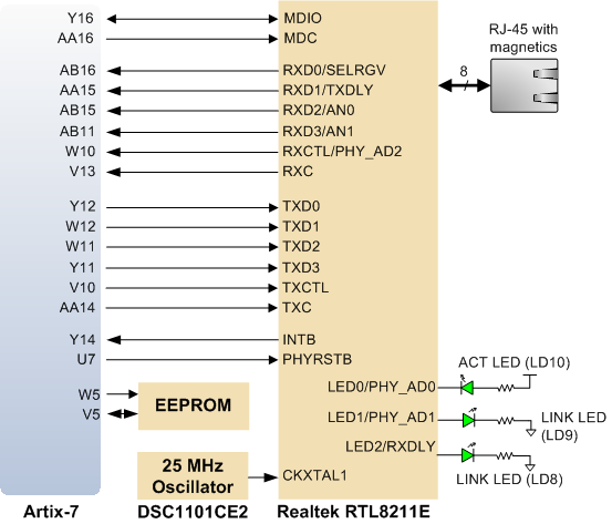 Figure 4. Pin connections between the Artix-7 and the Ethernet PHY.
5. Oscillators/Clocks
The Nexys Video board includes a single 100 MHz crystal oscillator connected to pin R4 (R4 is a MRCC input on bank 34). The input clock can drive MMCMs or PLLs to generate clocks of various frequencies and with known phase relationships that may be needed throughout a design. Some rules restrict which MMCMs and PLLs may be driven by the 100 MHz input clock. For a full description of these rules and of the capabilities of the Artix-7 clocking resources, refer to the “7-Series FPGAs Clocking Resources User Guide” (ug472) available from Xilinx.
Xilinx offers the Clocking Wizard IP core to help users generate the different clocks required for a specific design. This wizard will properly instantiate the needed MMCMs and PLLs based on the desired frequencies and phase relationships specified by the user. The wizard will then output an easy-to-use wrapper component around these clocking resources that can be inserted into the user's design. The clocking wizard can be accessed from within the Vivado Block Design or Core Generator tools.
6. USB UART Bridge (Serial Port)
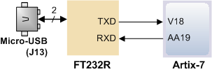
The Nexys Video includes an FTDI FT232R USB-UART bridge (attached to connector J13) that lets you use PC applications to communicate with the board using standard Windows COM port commands. Free USB-COM port drivers, available from Windows Update or www.ftdichip.com under the “Virtual Com Port” or VCP heading, convert USB packets to UART/serial port data. Serial port data is exchanged with the FPGA using a two-wire serial port (TXD/RXD) with no handshake signals. After the drivers are installed, I/O commands can be used from the PC directed to the COM port to produce serial data traffic on the V18 and AA19 FPGA pins.
Two on-board status LEDs provide visual feedback on traffic flowing through the port: the transmit LED (LD13) and the receive LED (LD12). Signal names that imply direction are from the point-of-view of the DTE (Data Terminal Equipment), in this case the PC.
The connections between the FT232R and the Artix-7 are shown in Fig. 5.
Figure 5. Nexys Video FT232R connections.
7. PC – FPGA Data Transfer (DPTI / DSPI)
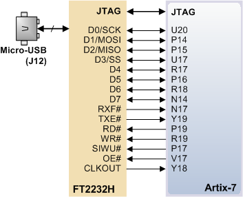
The Nexys Video provides two interface types that can be used to transfer user data between a PC and an FPGA design. Both of the interfaces have a software component, a Digilent Adept API, and a physical interface between the FPGA and the USB controller. Calling API functions on the PC will either present or request data on the FPGA pins according to the chosen protocol. The functionality is implemented using the on-board dual-port FT2232 USB controller. One port is used exclusively for JTAG, while the other either DPTI or DSPI. Since the interfaces share pins, DPTI and DSPI cannot be used simultaneously.
Figure 6. USB-FPGA interfaces provided by the USB PROG port.
7.1. Parallel Transfer Interface (DPTI)
DPTI is an 8-bit wide parallel FIFO-style data interface that offers higher bandwidth than DSPI. In FTDI-terminology, DPTI is equivalent to “FT245-style Asynchronous or Synchronous FIFO Interface”. It is available in both synchronous and asynchronous modes, configurable from the DPTI API. In synchronous mode, data transfer is timed by the clock provided by the USB controller that is input to the FPGA. In asynchronous mode, data transfer is happening on transitions of read and write control signals. The USB controller emulates a FIFO memory, providing status signals about the availability of data to be read or free space for data to be written. The FPGA controls data transfer by read, write, and output enable signals.
| Signal | Direction (FPGA) | Description |
|---|---|---|
| D[7:0] | I/O | Data bus. |
| RXF# | Input | When low, data is available for reading from the FIFO. |
| TXE# | Input | When low, data can be written to the FIFO. |
| RD# | Output | A low-pulse triggers data to be read out from the FIFO. |
| WR# | Output | A low-pulse triggers data to be written to the FIFO. |
| SIWU# | Input | Send immediate or Wake-up function. In normal mode a low-pulse triggers sending a data packet with the data currently in the FIFO, even if below the normal packet size. In suspend mode a low-pulse can wake up the Host PC. |
| OE# | Output | When low, the data bus is driven by the USB controller (read transfer). When high, the bus is driven by the FPGA (write transfer). |
| CLKO | Input | 60 MHz clock used in synchronous mode. Data is launched and can be captured on the rising edge. |
Table 5. DPTI signal description.
For more information, see the FT2232H data sheet.
7.2. Serial Peripheral Interface (DSPI)
An industry-standard SPI interface can also be used for transferring data. It uses only four signals for serial full-duplex communication. The USB controller acts as a SPI master, with the FPGA taking the slave role. The USB controller initiates a transaction after API function calls are made and transfers data in both directions simultaneously.
| Signal | Direction (FPGA) | Description |
|---|---|---|
| SCK | Input | Data bus. |
| MOSI | Output | When low, data is available for reading from the FIFO. |
| MISO | Input | When low, data can be written to the FIFO. |
| SS | Input | A low-pulse triggers data to be read out from the FIFO. |
Table 6. DSPI signal description.
For more information, see the FT2232H data sheet.
8. USB HID Host
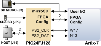
The Auxiliary Function microcontroller (Microchip® PIC24FJ128) provides the Nexys Video with USB HID host capability. After power-up, the microcontroller is in configuration mode, either downloading a bitstream to the FPGA, or waiting on it to be programmed from other sources. Once the FPGA is programmed, the microcontroller switches to application mode, which is USB HID Host in this case. Firmware in the microcontroller can drive a mouse or a keyboard attached to the type A USB connector at J15 labeled “USB Host.” Hub support is not currently available, so only a single mouse or a single keyboard can be used. The PIC24 drives several signals into the FPGA – two are used to implement a standard PS/2 interface for communication with a mouse or keyboard, and the others are connected to the FPGA's two-wire serial programming port, so the FPGA can be programmed from a file stored on a USB pen drive or microSD card.
Figure 7. Nexys Video PIC24 connections.
8.1. HID Controller
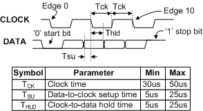
The Auxiliary Function microcontroller hides the USB HID protocol from the FPGA and emulates an old-style PS/2 bus. The microcontroller behaves just like a PS/2 keyboard or mouse would. This means new designs can re-use existing PS/2 IP cores. Mice and keyboards that use the PS/2 protocol use a two-wire serial bus (clock and data) to communicate with a host. On the Nexys Video, the microcontroller emulates a PS/2 device, while the FPGA plays the role of the host. Both the mouse and the keyboard use 11-bit words that include a start bit, data byte (LSB first), odd parity, and stop bit, but the data packets are organized differently, and the keyboard interface allows bi-directional data transfers (so the host device can illuminate state LEDs on the keyboard). Bus timings are shown in Fig. 8.
Figure 8. PS/2 device-to-host timing diagram.
The clock and data signals are only driven when data transfers occur; otherwise, they are held in the idle state at logic '1'. This requires that when the PS/2 signals are used in a design, internal pull-ups must be enabled in the FPGA on the data and clock pins. The clock signal is normally driven by the device, but may be held low by the host in special cases. The timings define signal requirements for mouse-to-host communications and bi-directional keyboard communications. A PS/2 interface circuit can be implemented in the FPGA to create a keyboard or mouse interface.
When a keyboard or mouse is connected to the Nexys Video, a “self-test passed” command (0xAA) is sent to the host. After this, commands may be issued to the device. Since both the keyboard and the mouse use the same PS/2 port, one can tell the type of device connected using the device ID. This ID can be read by issuing a Read ID command (0xF2). Also, a mouse sends its ID (0x00) right after the “self-test passed” command, which distinguishes it from a keyboard.
8.2. Keyboard
PS/2 uses open-collector drivers so the keyboard, or an attached host device, can drive the two-wire bus (if the host device will not send data to the keyboard, then the host can use input-only ports).
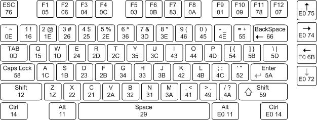
PS/2-style keyboards use scan codes to communicate key press data. Each key is assigned a code that is sent whenever the key is pressed. If the key is held down, the scan code will be sent repeatedly about once every 100ms. When a key is released, an F0 key-up code is sent, followed by the scan code of the released key. If a key can be shifted to produce a new character (like a capital letter), then a shift character is sent in addition to the scan code, and the host must determine which ASCII character to use. Some keys, called extended keys, send an E0 ahead of the scan code (and they may send more than one scan code). When an extended key is released, an E0 F0 key-up code is sent, followed by the scan code. Scan codes for most keys are shown in Fig. 9.
Figure 9. Keyboard scan codes.
A host device can also send data to the keyboard. Table 7 shows a list of some common commands a host might send.
| Command | Action |
|---|---|
| ED | Set Num Lock, Caps Lock, and Scroll Lock LEDs. Keyboard returns FA after receiving ED, then host sends a byte to set LED status: bit 0 sets Scroll Lock, bit 1 sets Num Lock, and bit 2 sets Caps lock. Bits 3 to 7 are ignored. |
| EE | Echo (test). Keyboard returns EE after receiving EE. |
| F3 | Set scan code repeat rate. Keyboard returns F3 on receiving FA, then host sends second byte to set the repeat rate. |
| FE | Resend. FE directs keyboard to re-send most recent scan code. |
| FF | Reset. Resets the keyboard. |
Table 7. Keyboard commands
The keyboard can send data to the host only when both the data and clock lines are high (or idle). Because the host is the bus master, the keyboard must check to see whether the host is sending data before driving the bus. To facilitate this, the clock line is used as a “clear to send” signal. If the host drives the clock line low, the keyboard must not send any data until the clock is released. The keyboard sends data to the host in 11-bit words that contain a '0' start bit, followed by 8-bits of scan code (LSB first), followed by an odd parity bit, and terminated with a '1' stop bit. The keyboard generates 11 clock transitions (at 20 to 30 KHz) when the data is sent, and data is valid on the falling edge of the clock.
8.3. Mouse
Once entered in stream mode and data reporting enabled, the mouse outputs a clock and data signal when it is moved; otherwise, these signals remain at logic '1.' Each time the mouse is moved, three 11-bit words are sent from the mouse to the host device, as shown in Fig. 10. Each of the 11-bit words contains a '0' start bit, followed by 8 bits of data (LSB first), followed by an odd parity bit, and terminated with a '1' stop bit. Thus, each data transmission contains 33 bits, where bits 0, 11, and 22 are '0' start bits, and bits 11, 21, and 33 are '1' stop bits. The three 8-bit data fields contain movement data as shown in the figure above. Data is valid at the falling edge of the clock, and the clock period is 20 to 30 KHz.
The mouse assumes a relative coordinate system wherein moving the mouse to the right generates a positive number in the X field, and moving to the left generates a negative number. Likewise, moving the mouse up generates a positive number in the Y field, and moving down represents a negative number (the XS and YS bits in the status byte are the sign bits – a '1' indicates a negative number). The magnitude of the X and Y numbers represent the rate of mouse movement: the larger the number, the faster the mouse is moving (the XV and YV bits in the status byte are movement overflow indicators – a '1' means overflow has occurred). If the mouse moves continuously, the 33-bit transmissions are repeated every 50ms or so. The L and R fields in the status byte indicate Left and Right button presses (a '1' indicates the button is being pressed).
The microcontroller also supports Microsoft® IntelliMouse®-type extensions for reporting back a third axis representing the mouse wheel, as shown in Table 8.
| Command | Action |
|---|---|
| EA | Set stream mode. The mouse responds with “acknowledge” (0xFA) then resets its movement counters and enters stream mode. |
| F4 | Enable data reporting. The mouse responds with “acknowledge” (0xFA) then enables data reporting and resets its movement counters. This command only affects behavior in stream mode. Once issued, mouse movement will automatically generate a data packet. |
| F5 | Disable data reporting. The mouse responds with “acknowledge” (0xFA) then disables data reporting and resets its movement counters. |
| F3 | Set mouse sample rate. The mouse responds with “acknowledge” (0xFA) then reads one more byte from the host. This byte is then saved as the new sample rate, and a new “acknowledge” packet is issued. |
| FE | Resend. FE directs mouse to re-send last packet. |
| FF | Reset. The mouse responds with “acknowledge” (0xFA) then enters reset mode. |
Table 8. Microsoft Intellimouse type extensions, commands and actions
9. Basic I/O
The Nexys Video board includes eight slide switches, five push buttons, and eight individual LEDs. The pushbuttons and slide switches are connected to the FPGA via series resistors to prevent damage from inadvertent short circuits (a short circuit could occur if an FPGA pin assigned to a pushbutton or slide switch was inadvertently defined as an output). The five pushbuttons arranged in a plus-sign configuration are “momentary” switches that normally generate a low output when they are at rest, and a high output only when they are pressed. The red pushbutton labeled “CPU RESET,” on the other hand, generates a high output when at rest and a low output when pressed. The CPU RESET button is intended to be used in processor designs to reset the processor, but you can also use it as a general purpose pushbutton. Slide switches generate constant high or low inputs depending on their position.
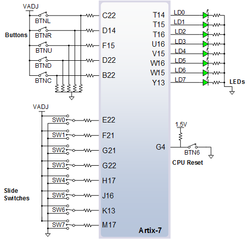 Figure 11. General purpose I/O connections.
The eight individual high-efficiency LEDs are anode-connected to the FPGA via 100-ohm resistors, so they will turn on when a logic high voltage is applied to their respective I/O pin. Additional LEDs that are not user-accessible indicate power-on, FPGA programming status, and USB and Ethernet port status.
10. Pmod Ports
The Pmod ports are arranged in a 2×6 right-angle, 100-mil female connectors that mate with standard 2×6 pin headers. Each 12-pin Pmod connector provides two power pins (6 and 12), two ground pins (5 and 11), and eight logic signals, as shown in Fig. 20. The VCC and Ground pins can deliver up to 1A of current. Pin assignments for the Pmod I/O connected to the FPGA are shown in Fig. 12.
Warning: Since the Pmod pins are connected to Artix-7 FPGA pins using a 3.3V logic standard, care should be taken not to drive these pins over 3.4V.
Figure 12. PMOD Ports: Front view as loaded on PCB.
The Nexys Video features four Pmod ports of different “styles” with subtle differences between them. Table 9 summarizes these differences.
| Pmod connector | Power | Analog/Digital | Routing | Series protection | Recommended usage |
|---|---|---|---|---|---|
| JXADC | VADJ | Dual | Differential; Pairs: 1-7,2-8,3-9,4-10 | 100 ohm | Analog inputs; input/output (VADJ=2.5V) |
| JA | 3.3 V | Digital-only | Single-ended | 200 ohm | <10 MHz, LVCMOS33 |
| JB, JC | 3.3 V | Digital-only | Differential; Pairs: 1-2,3-4,7-8,9-10 | 0 ohm | >=10MHz; LVDS_25 input only, or TMDS_33 input/output |
Table 9. Pmod differences
JXADC is a dual digital/analog Pmod wired to auxiliary analog FPGA input pins (see description below). JA, JB and JC are digital-only but routed in a different manner. JA signal traces are routed as single-ended signals with no length matching or characteristic impedance guarantees. JB and JC connector signals, on the other hand, are routed differentially in pairs at 100 ohm characteristic impedance. Inter-pair matching is +- 20mm. The series resistor on these two Pmods are replaced by 0 ohm shunts, so care must be exercised not to use voltages higher than 3.3V, or short FPGA-driven pins.
For slow, single-ended digital signals below 10 MHz, all Pmod ports are equivalent, assuming VADJ is set to 3.3 V (see the Power Supplies section). For higher frequencies, the routing and series protection need to be taken into account as well.
| PMOD Pinouts | |||
|---|---|---|---|
| JA1: AB22 | JB1: V9 | JC1: Y6 | JXADC1: J14 |
| JA2: AB21 | JB2: V8 | JC2: AA6 | JXADC2: H13 |
| JA3: AB20 | JB3: V7 | JC3: AA8 | JXADC3: G15 |
| JA4: AB18 | JB4: W7 | JC4: AB8 | JXADC4: J15 |
| JA7: Y21 | JB7: W9 | JC7: R6 | JXADC7: H14 |
| JA8: AA21 | JB8: Y9 | JC8: T6 | JXADC8: G13 |
| JA9: AA20 | JB9: Y8 | JC9: AB7 | JXADC9: G16 |
| JA10: AA18 | JB10: Y7 | JC10: AB6 | JXADC10: H15 |
Table 10. Nexys Video Pmod pin assignments.
Digilent produces a large collection of Pmod accessory boards that can attach to the Pmod expansion connectors to add ready-made functions like A/Ds, D/As, motor drivers, sensors, and other functions. Visit Digilent's website and check out the Pmod category for more information.
10.1. Dual Analog/Digital Pmod
The on-board Pmod expansion connector labeled “JXADC” is wired to the auxiliary analog input pins of the FPGA. Depending on the configuration, this connector can be used to input differential analog signals to the analog-to-digital converter inside the Artix-7 (XADC). Any or all pairs in the connector can be configured either as analog input or digital input-output.
The Dual Analog/Digital Pmod on the Nexys Video differs from the rest in the routing of its traces. The eight data signals are grouped into four pairs, with the pairs routed closely coupled for better analog noise immunity. Furthermore, each pair has a partially loaded anti-alias filter (100 ohm, 1 nF) laid out on the PCB. The filter does not have capacitors C5, C8, C9, and C10. In designs where such filters are desired, the capacitors can be manually loaded by the user.
NOTE: The coupled routing and the anti-alias filters might limit the data speeds when used for digital signals.
The XADC core within the Artix-7 is a dual channel 12-bit analog-to-digital converter capable of operating at 1 MSPS. Either channel can be driven by any of the auxiliary analog input pairs connected to the JXADC header. The XADC core is controlled and accessed from a user design via the Dynamic Reconfiguration Port (DRP). The DRP also provides access to voltage monitors that are present on each of the FPGA's power rails, and a temperature sensor that is internal to the FPGA. For more information on using the XADC core, refer to the Xilinx document titled “7 Series FPGAs and Zynq-7000 All Programmable SoC XADC Dual 12-Bit 1 MSPS Analog-to-Digital Converter User Guide” (ug480). A simple reference project that uses the XADC core can be found on the Nexys Video Resource Center.
11. Low Pin Count FMC Connector
The Nexys Video includes an FPGA mezzanine card (FMC) standard-conforming carrier card connector that enables connecting mezzanine modules compliant with the same standard. Nexys Video-based designs can now be easily extended with custom or off-the-shelf high-performance modules.
The actual connector used is a Samtec ASP-134603-01, the low-pin count, 10mm stacking height variant of the standard. It wires 34 differential pairs to regular FPGA user I/O pins powered by a voltage supply (VADJ) adjustable in the 1.2V-3.3V range. It also wires a 1 gigabit transceiver lane and its accompanying clock, the JTAG chain and auxiliary signals, and various voltage rails required by the standard. Thanks to the flexible voltage range supported by the Nexys Video, it allows high compatibility with existing and future FMC modules. It essentially allows the full range of I/O standards supported by the Artix-7 I/O architecture over the FMC connector. The FPGA can even be programmed to recognize the capabilities of a connected module and change the VADJ voltage on-the-fly.
The pinout of the FMC connector can be found in the UCF/XDC constraints file available on the Nexys Video Resource Center.
The gigabit transceiver lane includes a receive pair, a transmit pair, and a reference clock input to the FPGA, all going to MGT bank 216. The transceiver lane is wired to lane 3 (GTPE2_CHANNEL_X0Y7). The reference clock is wired to REFCLK1 of the same bank (GTPE2_COMMON_X0Y1). It is important to keep in mind that bank 216, being the only one available in this FPGA package, is shared between the DisplayPort source and FMC ports. Depending on the exact application, simultaneous usage of the FMC gigabit lane and DisplayPort might not be possible. Regular FMC I/O signals are not affected.
12. MicroSD Slot
The Nexys Video provides a microSD slot for both FPGA configuration and user access. The on-board Auxiliary Function microcontroller shares the SD card bus with the FPGA. Before the FPGA is configured, the microcontroller must have access to the SD card via SPI interface. Once a bit file is downloaded to the FPGA (from any source), the microcontroller powers off the SD slot and relinquishes control of the bus. The FPGA design will find the SD card in an unpowered state.
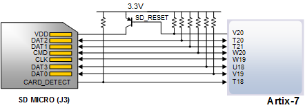
All of the SD pins on the FPGA are wired to support full SD speeds in native interface mode, as shown in Fig. 12. The SPI interface is also available, if needed. Once control over the SD bus is passed from the microcontroller to the FPGA, the SD_RESET signal needs to be actively driven low by the FPGA to power the microSD card slot. For information on implementing an SD card controller, refer to the SD card specification available at www.sdcard.org.
Figure 13. Artix-7 microSD card connector interface (PIC24 connections not shown).
13. HDMI
The Nexys Video board contains two buffered HDMI ports: one source port J8 (output), and one sink port J9 (input). Both ports use HDMI type-A receptacles and include an HDMI buffer: An AD8195 buffer for input and a TMDS141 for output. The buffers work by terminating, equalizing, conditioning, and forwarding the HDMI stream between the connector and FPGA pins.
Both HDMI and DVI systems use the same TMDS signaling standard, directly supported by Artix-7 user I/O infrastructure. Also, HDMI sources are backward compatible with DVI sinks, and vice versa. Thus, simple passive adaptors (available at most electronics stores) can be used to drive a DVI monitor or accept a DVI input. The HDMI receptacle only includes digital signals, so only DVI-D mode is possible.
The 19-pin HDMI connectors include three differential data channels, one differential clock channel five GND connections, a one-wire Consumer Electronics Control (CEC) bus, a two-wire Display Data Channel (DDC) bus that is essentially an I2C bus, a Hot Plug Detect (HPD) signal, a 5V signal capable of delivering up to 50mA, and one reserved (RES) pin. All are wired to the FPGA with the exception of RES.
| Pin/Signal | J8 (source) | J9 (sink) | ||
|---|---|---|---|---|
| Description | FPGA pin | Description | FPGA pin | |
| D[2]_P, D[2]_N | Data output | AB3, AB2 | Data input | U2, V2 |
| D[1]_P, D[1]_N | Data output | AA1, AB1 | Data input | W2, Y2 |
| D[0]_P, D[0]_N | Data output | W1, Y1 | Data input | Y3, AA3 |
| CLK_P, CLK_N | Clock output | T1, U1 | Clock input | V4, W4 |
| CEC | Consumer Electronics Control bidirectional | AA4 | Consumer Electronics Control bidirectional | AA5 |
| SCL, SDA | DDC bidirectional | U3, V3 | DDC bidirectional | Y4, AB5 |
| HPD/HPA | Hot-plug detect input | AB13 | Hot-plug assert output | AB12 |
| 5V0 | Powered from 5V rail | N/A | Powers auxiliary signals | N/A |
| TXEN | Transmitter enable output | R3 | ||
Table 11. HDMI pin description and assignment.
13.1 TMDS Signals
HDMI/DVI is a high-speed digital video stream interface using transition-minimized differential signaling (TMDS). To make proper use of either of the HDMI ports, a standard-compliant transmitter or receiver needs to be implemented in the FPGA. The implementation details are outside the scope of this manual. Check out the Nexys Video Resource Center for ready-to-use reference IP.
13.2 Auxiliary signals
A pull-down resistor on the TXEN signal makes sure the sink buffer's transmitter facing the FPGA is disabled by default. An FPGA design using the sink port needs to actively drive this pin high for the buffer to pass data through.
Whenever a sink is ready and wishes to announce its presence, it connects the 5V0 supply pin to the HPD pin. On the Nexys Video, this is done by driving the Hot Plug Assert signal high. Note this should only be done after a DDC channel slave has been implemented in the FPGA and is ready to transmit display data.
The Display Data Channel, or DDC, is a collection of protocols that enable communication between the display (sink) and graphics adapter (source). The DDC2B variant is based on I2C, the bus master being the source and the bus slave the sink. When a source detects high level on the HPD pin, it queries the sink over the DDC bus for video capabilities. It determines whether the sink is DVI or HDMI-capable and what resolutions are supported. Only afterwards will video transmission begin. Refer to VESA E-DDC specifications for more information.
The Consumer Electronics Control, or CEC, is an optional protocol that allows control messages to be passed around on an HDMI chain between different products. A common use case is a TV passing control messages originating from a universal remote to a DVR or satellite receiver. It is a one-wire protocol at 3.3V level connected to an FPGA user I/O pin. The wire can be controlled in an open-drain fashion allowing for multiple devices sharing a common CEC wire. Refer to the CEC addendum of HDMI 1.3 or later specifications for more information.
14. DisplayPort Output
DisplayPort is a relatively new industry standard for digital display technology. Its advantages over existing technologies are: higher bandwidth for greater resolutions and color depths, bi-directional auxiliary channel, variable interface width, and flexible power topologies, among others.
DisplayPort defines a high-speed main link carrying audio and video data, an auxiliary channel, and a hot-plug detect signal. The main link is a uni-directional, high-bandwidth and low-latency channel. It consists of one, two, or four AC-coupled differential pairs, called lanes. Version 1.1 of the standard defines two link rates: 1.62 and 2.7 Gbps. The lanes carry both data and an embedded clock at the link rate negotiated between Source and Sink, independent of the resolution and color depth of the video stream. The link rate is de-coupled from the pixel rate, resulting in a packetized stream. This differentiates DisplayPort from other digital video standards, like DVI/HDMI. Due to the high link rate, the main link can only be implemented on dedicated gigabit transceiver pins of the Artix-7 architecture.
The auxiliary channel is a bidirectional channel for link management and device control. It is AC-coupled, just like the main link lanes, but uses a different encoding and the lower data rate of 1Mbps. Upon hot-plug detection, a Source will attempt to configure the link through link training. Handshaking link parameters happens via the auxiliary channel.
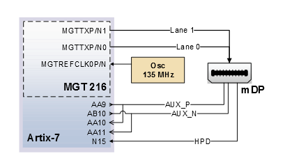
Nexys Video includes a Mini DisplayPort (mDP) connector wired in the Source role. The maximum lane count supported is two. The two lanes of the main link are wired to the only gigabit transceiver bank: MGT bank 216. Lane 0 is mapped to GTPE2_CHANNEL_X0Y4, while Lane 1 goes to GTPE2_CHANNEL_X0Y5. It is important to keep in mind that bank 216, being the only one available in this FPGA package, is shared between the DisplayPort source and FMC ports. Depending on the exact application, simultaneous usage of the FMC gigabit lane and DisplayPort might not be possible.
On-board there is a 135 MHz reference oscillator mapped to GTPE2_COMMON_X0Y1/MGTREFCLK1, which should be used to generate the desired link rate. Refer to the Xilinx 7 Series FPGAs GTP Transceivers user guide (ug482) for more information on how to implement high-speed interfaces.
The auxiliary channel is a bidirectional LVDS bus. Depending on the Xilinx tool/IP version, instantiating a differential I/O buffer with LVDS signaling standard might not be possible. The work-around is to have two pairs of pins wired and shorted together as seen in Fig. 14. One pair should be implemented as input-only and the other as output-only.
If the tool/IP allows bidirectional LVDS buffers, only one of the pairs needs to be used (it does not matter which), while the other declared as input and not used.
The hot-plug detect (HPD) signal connects to a general user I/O pin and should be configured as an input. It will be asserted when a sink is attached.
Figure 15. DisplayPort wiring diagram.
The full implementation details of the DisplayPort standard is outside the scope of this document. Refer to the full specifications published by VESA for more details.
Xilinx provides a fully documented Vivado IP core that implements a DisplayPort controller. Using this core will greatly decrease the development required to get DisplayPort working on the Nexys Video. This core requires a paid license, but a 120 day evaluation license can be obtained for free from the Xilinx website.
15. OLED
A Univision Technology Inc. UG-2832HSWEG04 is loaded on the Nexys Video. It is a white monochrome, 128 x 32, 0.91“ organic LED display matrix bundled with a Solomon Systech SSD1306 display controller. The display data interface towards the FPGA is a 4-wire serial peripheral interface (SPI). The 4 wires in controller-terminology are CS#, D/C#, SDIN, and SCLK, but CS# is hard-wired to ground. This adds to the reset and two power control signals for proper start-up sequencing. The signals are summarized in Table 11.
| Signal | Description | Polarity | FPGA pin |
|---|---|---|---|
| RES# | Reset | Active-low | U21 |
| CS# | Chip select (always active) | Active-low | N/A |
| D/C# | Data (high)/Command (low) | Both | W22 |
| SCLK | Serial Clock | Active-high | W21 |
| SDIN | Serial Data | Active-high | Y22 |
| VBAT# | Power enable for internal power supply | Active-low | P20 |
| VDD# | Power enable for digital power | Active-low | V22 |
Table 12. OLED signal description.
The serial interface is synchronous to SCLK and must conform to the timing specifications below. In most cases, a 10 MHz SCLK and data sent on the falling edge should work.
Figure 16. Serial interface timing diagram.
Figure 17. OLED serial interface bit ordering.
| Symbol | Parameter | Min | Typ. | Max | Unit |
|---|---|---|---|---|---|
| tcycle | Clock Cycle Time | 100 | - | - | ns |
| tAS | Address Setup Time | 15 | - | - | ns |
| tAH | Address Hold Time | 15 | - | - | ns |
| tCSS | Chip Select Setup Time | 20 | - | - | ns |
| tCSH | Chip Select Hold Time | 10 | - | - | ns |
| tDSW | Write Data Setup Time | 15 | - | - | ns |
| tDHW | Write Data Hold Time | 15 | - | - | ns |
| tCLKL | Clock Low Time | 20 | - | - | ns |
| tCLKH | Clock High Time | 20 | - | - | ns |
| tR | Rise Time | - | - | 40 | ns |
| tF | Fall Time | - | - | 40 | ns |
Table 13. Timing diagram symbols and parameters.
Start-up sequence:
- Power up VDD by pulling OLED_VDD low. Wait 1ms.
- Pulse RES# low for at least 3us.
- Send initialization/configuration commands (see Table 12).
- Power up VBAT by pulling OLED_VBAT low. Wait 100ms for voltage to stabilize.
- Clear screen by writing zero to the display buffer.
- Send “Display On” command (0xAF).
| Command function | Command bytes |
|---|---|
| Charge pump enable | 0x8D, 0x14 |
| Set pre-charge period | 0xD9, 0xF1 |
| Contrast control | 0x81, 0x0F |
| Column inversion disable | 0xA0 |
| Scan direction | 0xC0 |
| COM pins configuration | 0xDA, 0x00 |
| Addressing mode: horizontal | 0x20 |
Table 14. OLED configuration commands
After start-up, writing to the display is done by sending data bytes over the serial interface (D/C# high). Each data bit corresponds to a pixel with the addressing mode, inversion, and scan direction settings determining exactly which. Check out the Nexys Video Resource Center for reference projects that use the OLED.
16. Audio Codec
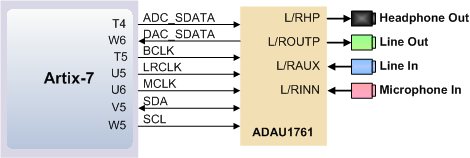
The Nexys Video board includes an Analog Devices ADAU1761 SigmaDSP audio codec (IC4) complementing its multimedia features. Four 1/8” (3.5mm) audio jacks are available for line-out (J5-green), headphone-out (J3-black), line-in (J7-blue), and microphone-in (J6-pink). Each jack carries two channels of analog audio (stereo), with the exception of the microphone input, which is mono.
To record or play back audio in an FPGA design, the audio data needs to be converted. The audio codec bridges the gap between the analog jacks and the digital FPGA pins. Analog-to-digital and digital-to-analog conversion is done at up to 24 bits and 96 kHz sampling rate. Digital audio data is carried to/from the FPGA on a serial, full-duplex interface which supports several different formats, the default being I2S. This interface is clocked by the FPGA through BCLK by default, but the codec can be configured to provide the clock itself.
Configuring the audio codec can be done over I2C. It responds to slave address 0b0111011, followed by a 16-bit register address and one or more data bytes. These registers control every functional aspect of the codec.
The codec is clocked from the FPGA through the Master Clock (MCLK) pin. A clock must be provided for the codec to function, including the I2C port. The exact frequency depends on the desired sample rate and whether PLL will be used, but 12 MHz is a good start. The clocking infrastructure of 7 series FPGA is more than capable of synthesizing the right frequency from the on-board 100 MHz reference oscillator.
For proper use, the concept of audio paths needs to be understood. There are two signal paths internal to the codec: Playback and Record. Both are highly configurable analog paths with mixers and amplifiers that route audio signals through the chip. The Playback path is the output path that routes audio from different sources, like the digital-to-analog converter or input mixers towards the headphone and line-out jacks. On the other hand, the record path routes audio from the line-in and microphone-in towards the analog-to-digital converters. Having routing elements at every step enables signal mixing between channels, amplification, muting, and bypass. However, it also means that each element has to be properly configured along the path.
Keep in mind that audio jack designations might differ from codec analog frontend designators. For example, the line-in jack connects to the AUX port of the codec. The microphone jack is wired to the IN port. Also, notice that although some ports offer differential amplifiers and signaling, they are not used on the Nexys Video. For example, the OUT port is differential, comprising 4 pins: LOUTP, LOUTN, ROUTP, and ROUTN. However, the N-side of the differential pairs is left floating, while the P-side connects to the jack.
At the very least, an audio-aware FPGA design should do the following:
- Provide MCLK for the audio codec.
- Use an I2C master controller to configure the core clocking, sample rates, serial interface format, and audio path.
- Send or receive audio samples over the serial audio data channel for playback or record.
A MicroBlaze based reference project that uses the audio codec is available on the Nexys Video Resource Center.
More advanced users might want to try additional features of the ADAU1761. For example, the on-chip SigmaDSP core can be programmed to do user-defined digital signal processing. All relevant information can be found in the ADAU1761 data sheet.
Figure 18. Audio signal connections.
| Signal Name | FPGA Pin | Pin Function |
|---|---|---|
| ADC_SDATA | T4 | Serialized audio resulting from the analog-to-digital conversion (record). |
| DAC_SDATA | W6 | Serialized audio is converted to analog by the codec (playback). |
| BCLK | T5 | Serial data port clock. |
| LRCLK | U5 | Serial data port frame clock. |
| MCLK | U6 | Master clock. |
| SDA | V5 | I2C configuration interface. |
| SCL | W5 | I2C configuration interface. |
Table 15. Audio signal description.
17. Out-of-box Demo
The Nexys Video comes with an out-of-box demo design that gets loaded from the on-board Quad SPI flash. It exercises most of the on-board peripherals. Follow the instructions to explore them all:
- Connecting an HDMI/DVI or DisplayPort monitor shows a test pattern with a mouse pointer.
- Connecting a USB mouse controls the mouse pointer on the display.
- Connecting an HDMI/DVI source, like a laptop output, replaces the test pattern with the source image.
- Connecting the board to an Ethernet network will acquire link, IP address, and become “pingable” at the IPv4 address displayed on the OLED.
- The internal XADC temperature is read and shown on the OLED.
- Connecting the USB-UART port to a PC and opening a terminal (115200,8,N,1) shows status messages.
- Pushing BTNU records audio off the microphone input for five seconds and plays it back on the headphone output if BTND is pushed, or line-out if BTNL. Similarly, BTNR starts a recording off the line-in jack.
- Slide switches are wired to the LEDs above.
The source code for this design is available on the Nexys Video Resource Center.

