Add a Processor to a Block Design
The process of adding a processor to your design is very different depending on the processor used. The Microblaze dropdown should be selected only if using a board that does not have a Zynq device.
- Add a Microblaze Processor to a Block Design
-
The Microblaze soft-core processor IP can be used to instantiate a processor within your FPGA design. This processor can be very useful for controlling and configuring hardware components. This section discusses how you can add a Microblaze processor and several useful components, including UART for standard output and DDR memory support, to your block design.
Note: This section is intended for use with boards without a Zynq chip. For Zynq boards, the Zynq7 Processing System should be used instead.
Note: If you aren't sure whether your board has DDR memory, check the Memory column of the specification table on this site's Programmable Logic page.
- Follow the steps in this dropdown for boards without DDR memory
-
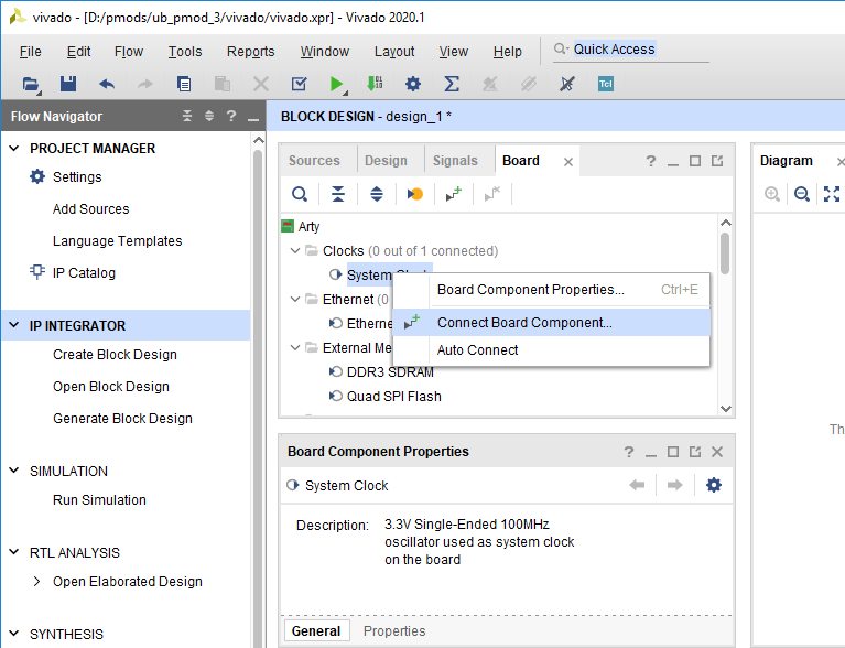
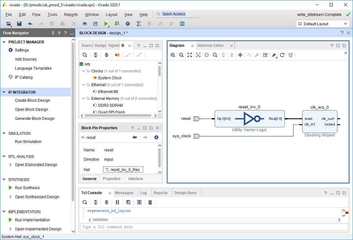
First, an external clock should be added to the block design, so that it can be used to generate any other clocks required by the design. Open the Board tab, and find the system clock. Right-click on it and select Connect Board Component.
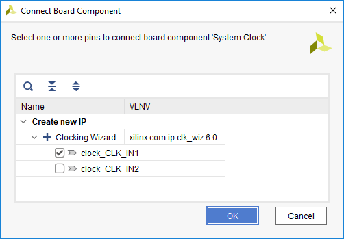
In the Connect Board Component dialog, select the CLK_IN1 of a new Clocking Wizard IP. This will add a clocking wizard to the design, which can be used to easily configure the board's MMCMs and PLLs to generate any required clocks. Click OK to continue.
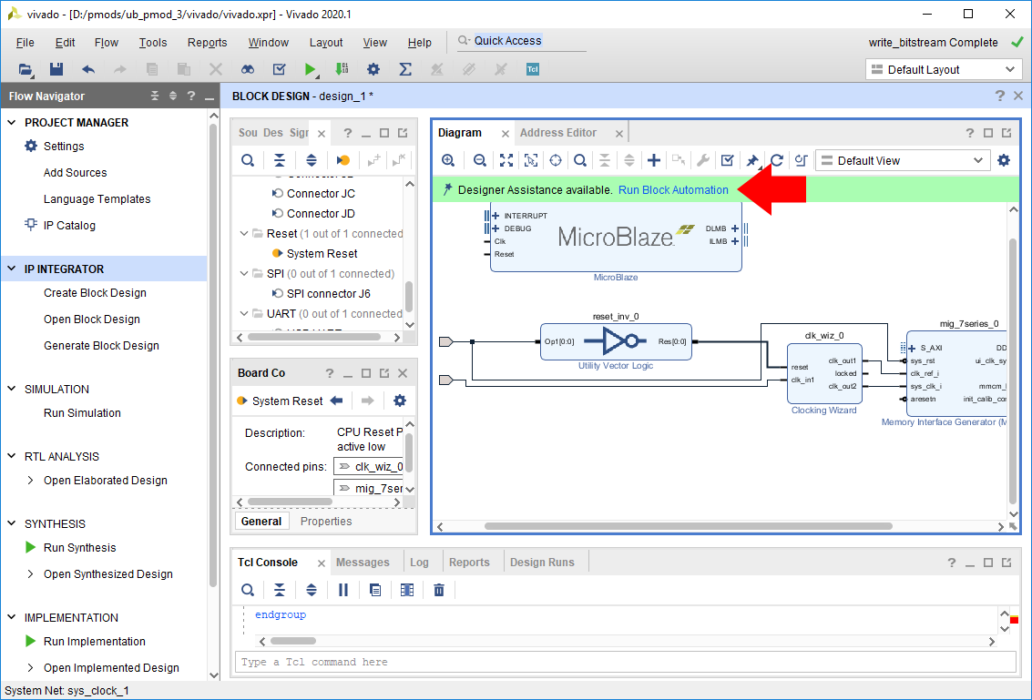
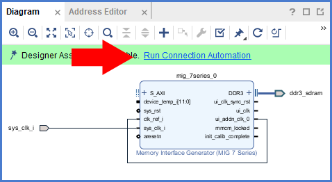
Next, an external reset port should be added to the design that can be used to reset the entire system. Click the Run Connection Automation button in the green Designer Assistance toolbar.
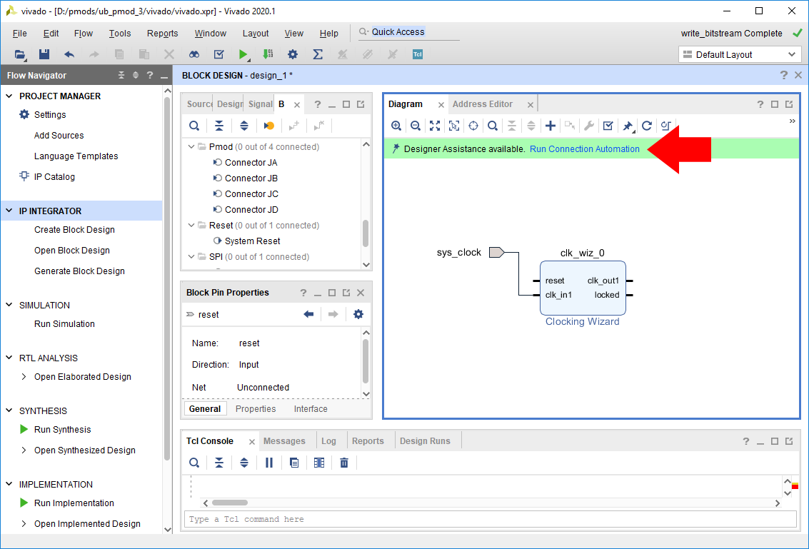
In the Run Connection Automation dialog, in the list on the left side of the dialog, make sure that the Clocking Wizard's reset box is checked. The Select Board Part Interface dropdown lists any options for resets that are specified in your board's board files. For most boards, only one option will be available. Click OK to continue.
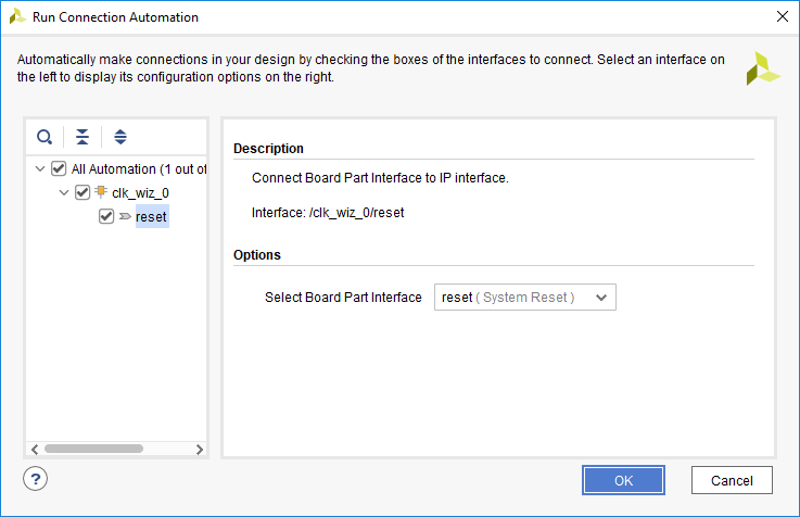
Note: Depending on the polarity of the reset button (active high or active low), a Utility Vector Logic IP may be inserted between the reset port and the Clocking Wizard. This is used to ensure that the active high reset pin of the IP is provided with the correct polarity of reset signal, and that the design will not be held in reset while the reset button is not pressed.
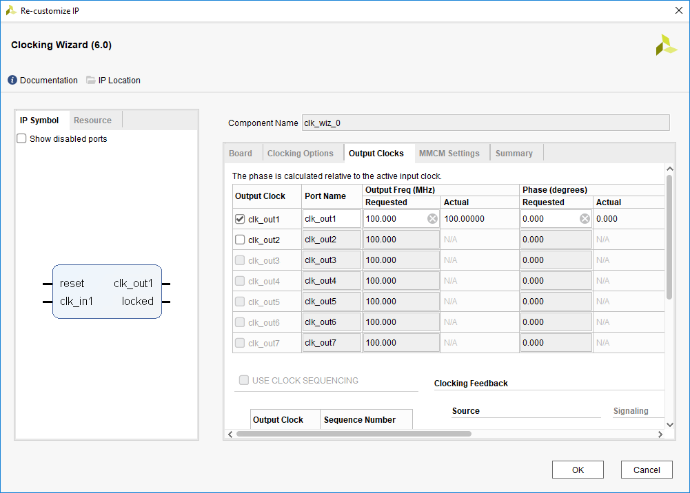
Your design will require at least one clock from the clocking wizard. If your design requires more clocks, then they must be added through the Clocking Wizard.
Double click on the Clocking Wizard IP core to edit its settings. Navigate to the Output Clocks tab. Additional clocks are added to the Clocking Wizard by checking a box in the Output Clock column, and specifying a Requested Output Frequency. Additionally, if desired, the ports can be named according to their intended purpose.
If your design requires additional clocks (such as for an ext_spi_clock pin), they should be added now.
Click OK to confirm your changes to the Clocking Wizard's settings.
If you aren't sure that you have all of the clocks you need, don't worry, you can always come back and add them by reconfiguring this IP. This task can be performed whenever in the design process it becomes necessary.
Next, use the Add IP button (
 ) to add the MicroBlaze IP to the design. The block that is added represents the core of the Microblaze processor.
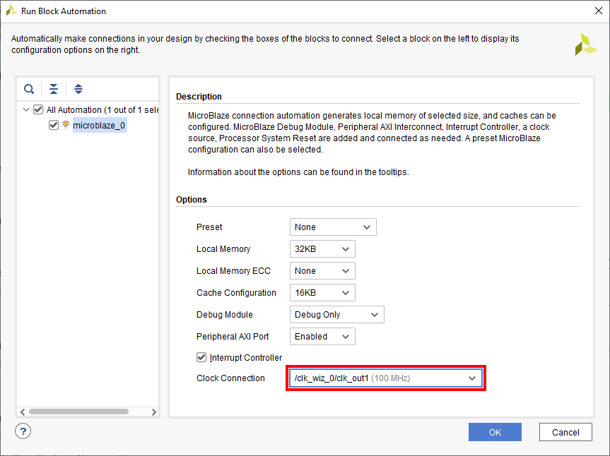
Next, block automation will be run so that additional supporting infrastructure can be added to the design. Click Run Block Automation in the green Designer Assistance bar.
Note: The screenshot to the right is not representative for a design not using DDR, as these designs will not contain a MIG IP core.
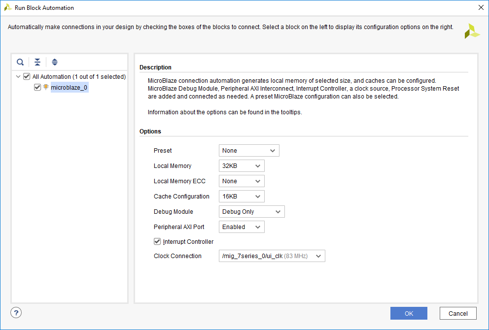
In the Run Block Automation dialog, several settings can be specified for how the Microblaze IP will be connected to the rest of the design:
- Local Memory specifies how much block RAM memory will be dedicated to the processor. DDR-less designs require more memory, and the amount of memory necessary depends heavily on the size of the software application being run. 32KB is enough for many small applications.
- Cache Configuration can help the speed of designs using DDR memory. It should be enabled when using DDR and disabled otherwise.
- Debug Module allows you to specify the capabilities of the debugger. The default Debug Only option is recommended.
- Peripheral AXI Port enables or disables the AXI master interface of the processor. It must be enabled to allow the processor to be connected to hardware peripherals.
- Interrupt Controller specifies whether the processor can be interrupted by its peripherals. Whether or not it needs to be enabled depends on your design requirements. If any IP that you intend to connect to the processor must have interrupts to function correctly, the box must be checked.
- Clock Connection specifies the processor's clock. Designs using DDR should use the MIG's ui_clk pin, while designs without DDR should use the Clocking Wizards clk_out1 pin.
Note: Settings not present in this list are out of the scope of this guide, and can safely be left as their default.
Confirm that the settings meet your design requirements. It should be noted that while it is possible to change these settings manually later (for example, by manually adding an AXI INTC IP and connecting it to the processor), the easiest way to do so will be to clear the Microblaze processor out of your block design and restart the process of adding the processor. This is to say, the settings chosen here are important. Getting them right the first time will save you time in the long run.
Click OK to continue.
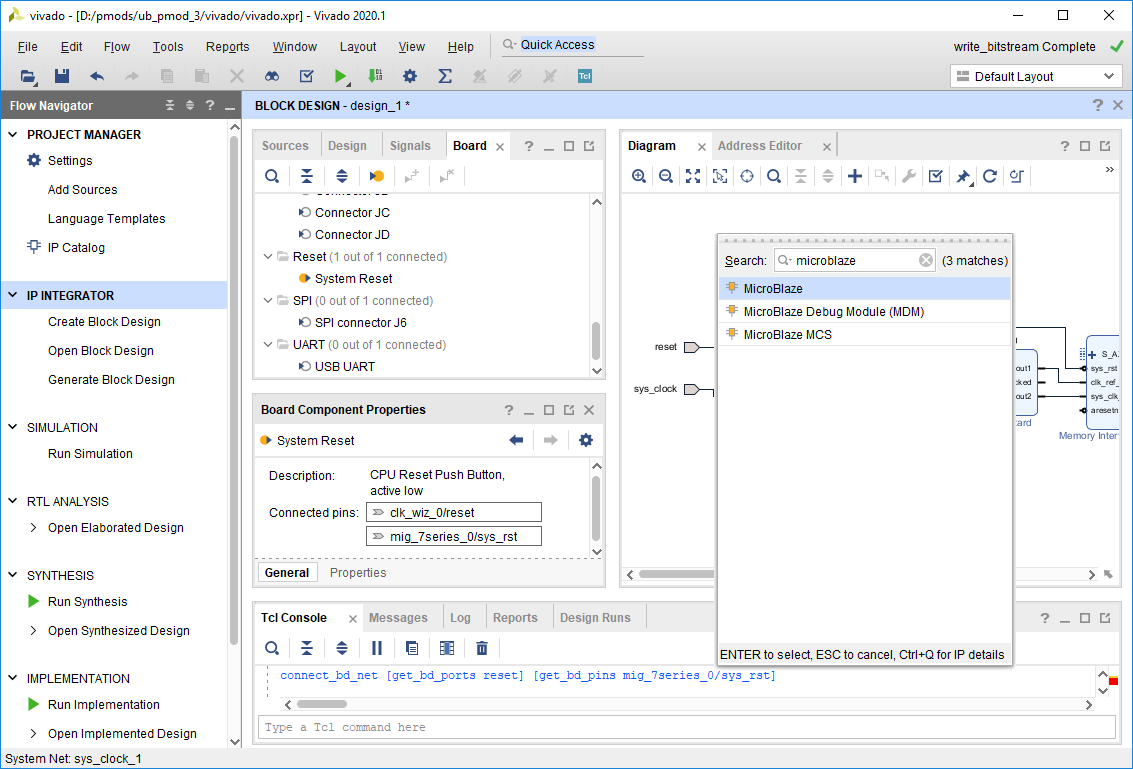
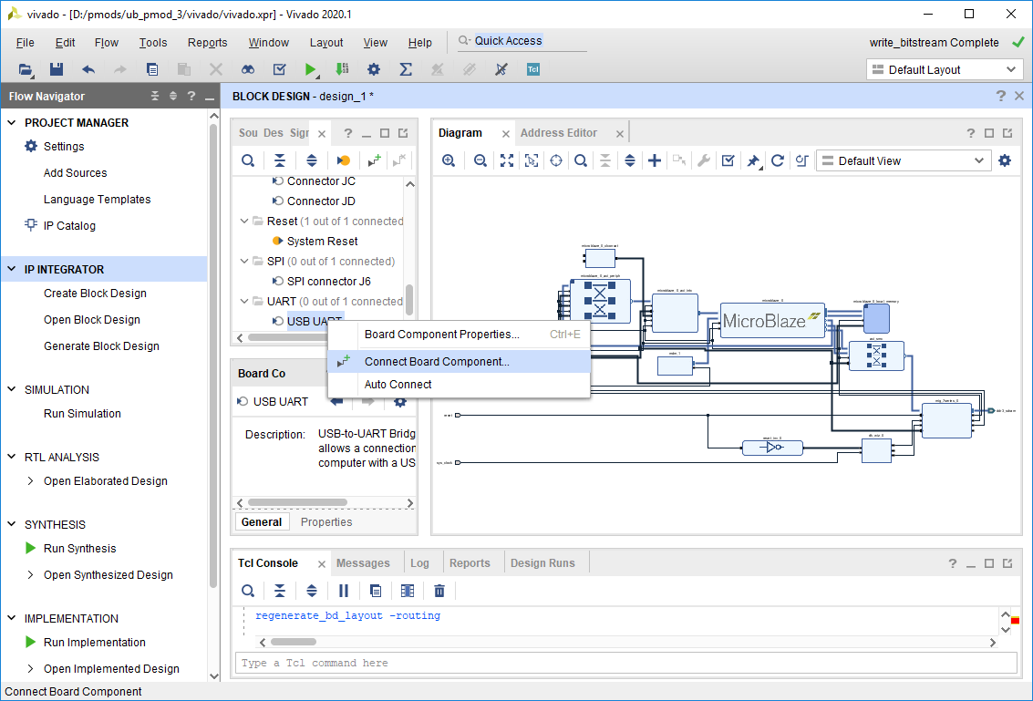
Next, in order for the software design to be able to print to a serial console on a host computer, a UART peripheral must be connected. Find the USB UART interface in the Board tab, right click on it, and select Connect Board Component.
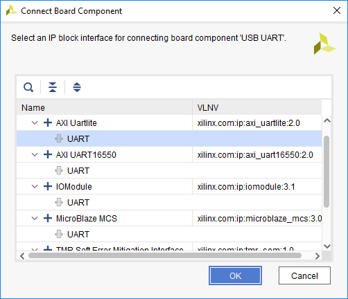
In the dialog that pops up, select a new AXI Uartlite IP's UART interface, and click OK to add the block to the diagram.
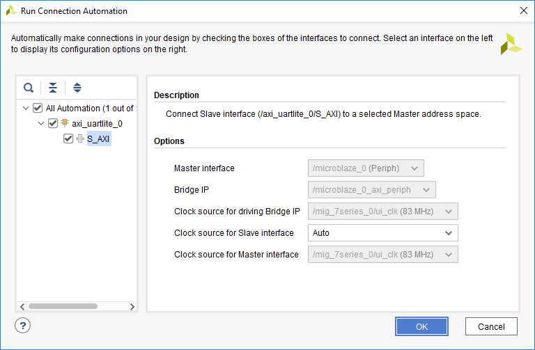
To connect all remaining AXI cores that have not yet been connected to the processor, click the Run Connection Automation button in the green Designer Assistance bar. Check the All Automation box in the list on the left side of the window to select all of the remaining AXI cores. The dropdown settings available for each core can safely be left as their default values. Click OK to automatically connect them to the processor.
- Follow the steps in this dropdown for boards with DDR memory
-
The user Viktor Nikolov posted a tutorial on the Digilent Forum with an alternate architecture for clocking the DDR interface for Digilent boards. It works around several errors that may occur in the flow presented here and is recommended for new users to go through. Digilent is considering updating this and other guides and reference material to use the revised flow. Find more information and a comprehensive guide here: https://forum.digilent.com/topic/27389-arty-a7-microblaze-ddr3-tutorial/.
When creating a design with DDR, it's best to add the DDR interface first, as it is typically also used to generate the clock or clocks that will be used by the rest of your design.
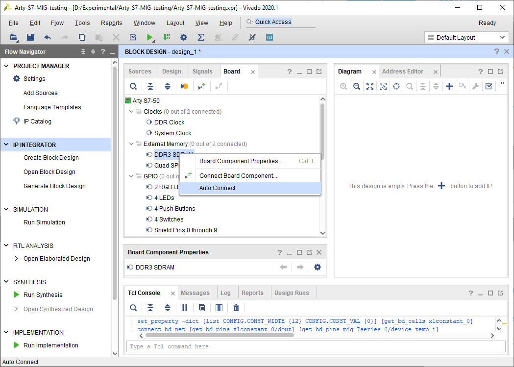
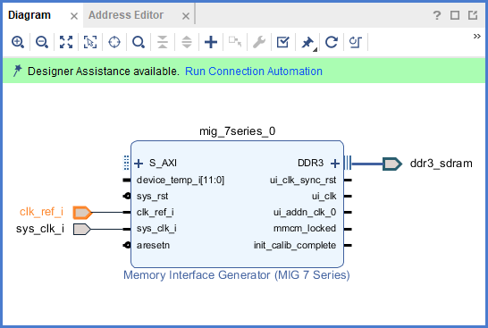
In the Board tab, right click on the DDR interface and select “Auto Connect”. This process will add a MIG (Memory Interface Generator) and the external DDR interface to the design. Two clock pins are also created, which will need to be modified.
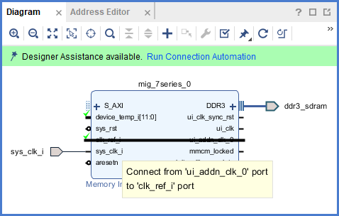
Delete the “clk_ref_i” pin. This can be accomplished either by right-clicking on the pin and selecting delete or by selecting and pressing the delete key.
Verify that the “ui_addn_clk_0” pin has a frequency near 200 MHz by selecting it and looking at the “Frequency” value in the “Block Pin Properties” pane.

Manually connect the “ui_addn_clk_0” pin to the “clk_ref_i” pin by clicking and dragging from one to the other.
It's important to note that the “sys_clk_i” pin will not be constrained by the board files, and you will need to add a constraint file to map it to the corresponding pin location on the FPGA.
If your project doesn't contain the master Xilinx Design Constraint (XDC) file for your board, the dropdown below details how to add it. This file contains the constraints that your board places on designs using it - specific interfaces wired up to specific pins, clock frequencies, and FPGA bank voltages, for some examples. Click the dropdown below for a walkthrough of how to add this file to your project.
- Add a Master XDC File to a Vivado Project
-
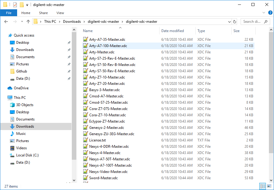
Download and extract digilent-xdc-master.zip. This file includes all of the latest template XDC files released for Digilent's boards, which are available on Github in the digilent-xdc repository.
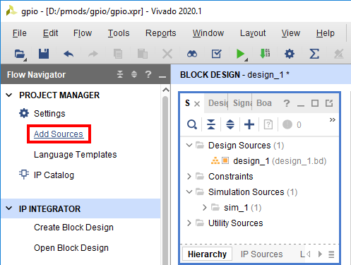
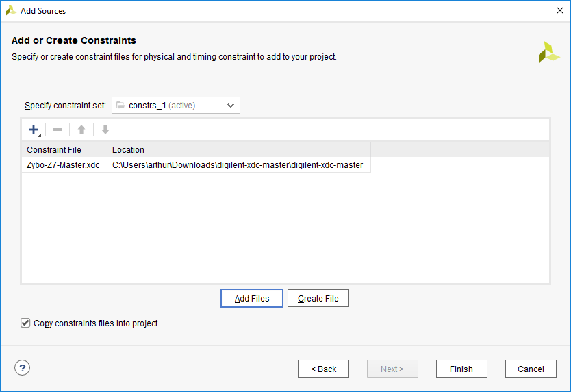
Returning to Vivado, click the Add Sources button in the Project Manager section of the Flow Navigator pane. This will launch a dialog that you can use to add a variety of types of source files to the project (or create new ones).
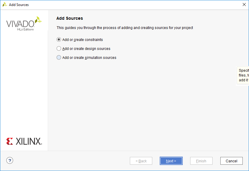
On the first screen, select Add or create constraints. Click Next to continue.
In the next screen, make sure that the constraint set specified (the one that the master XDC will be added to) is set to constrs_1, and that it is the active set. Click the Add Files button.

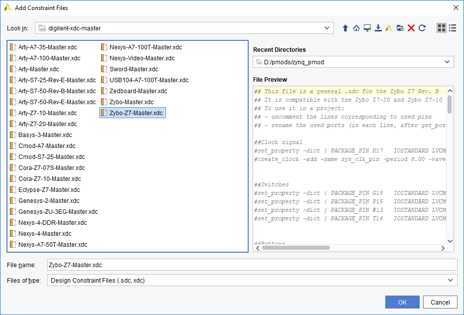
In the dialog that pops up, navigate to the folder that the digilent-xdc-master.zip file was extracted into. Highlight the XDC file for your board, then click OK to continue.
Back in the Add Sources dialog, make sure that your chosen constraint file appears in the table. Also, make sure that the Copy constraint files into project box is checked. If this box is unchecked, the file will be linked by your project, and any modifications made within the project will affect the version you downloaded. Since you may need to use this file again in other projects, copying the constraint file is recommended, so that you can always work from a fresh copy.
Click Finish to add the constraint file to your project.
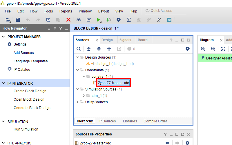
Once added, the XDC file will appear in the Sources tab (in the same pane as the Board tab). Double click it to open the file.
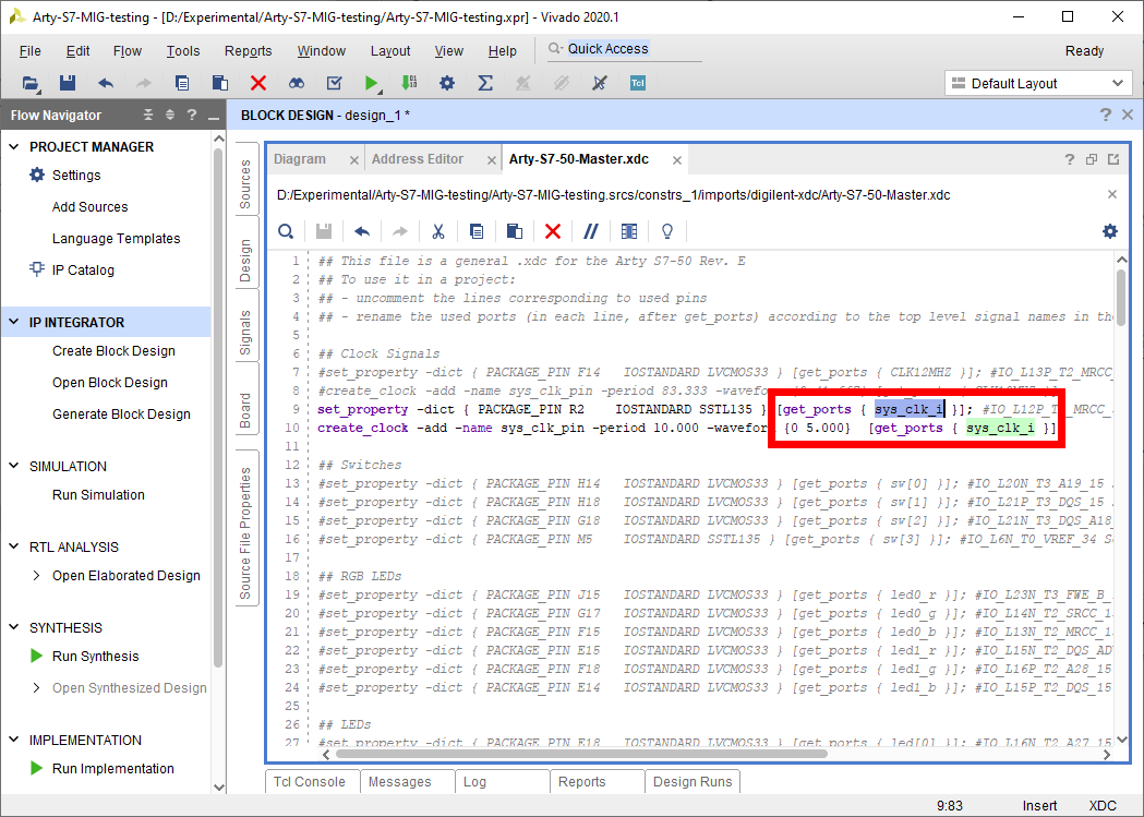
Find the set_property and create_clock constraints for your board's 100 MHz input clock, uncomment them by removing the
#at the start of each line, and change the name of the port that they are constraining tosys_clk_i, to match the name of the port in the block design.If your board has multiple clocks, the 100 MHz one can be determined by observing that the create_clock constraint specifies a
10.000ns period, as seen in the screenshot to the right.Make sure to save your changes.
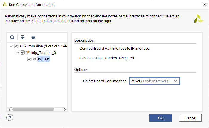
Next, the MIG's reset pin will be connected to the board's reset button. Click “Run Connection Automation” in the green bar at the top of the window.
In the list to the left side of the dialog that pops up, make sure that the “sys_rst” box is checked. Click OK to connect the reset to the corresponding board part interface.
The MIG block may have other ports which will need to be connected to ensure that it works correctly. This section discusses each of those ports.
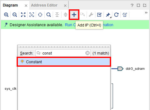
- Open this dropdown if your MIG has a "device_temp_i" port
-
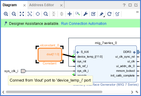
If your MIG block has a “device_temp_i” port, it means that the MIG is not using the chip's XADC analog-to-digital converter feature. We'll ground this port to prevent any warnings that it may throw. Add a “Constant” IP to the design.
Double click on the block to open it's configuration wizard and modify it to have a Value of “0” and a Width of “12”.

Connect its output port to the “device_temp_i” port on the MIG.
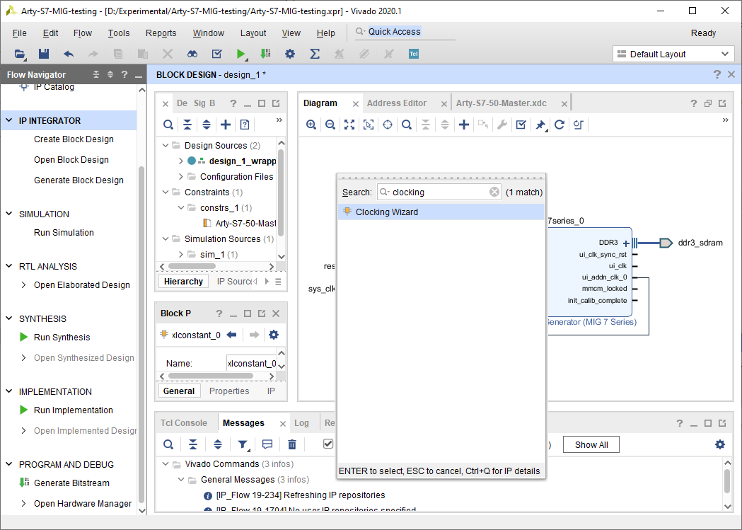
If your design requires more clocks than just the ui_clk provided by the MIG, you will need to add a clocking wizard IP that is driven by the MIG's ui_clk.
Use the Add IP button to search for and add a Clocking Wizard to the design.
Manually connect the Clocking Wizard's clk_in1 and reset ports to the MIG's ui_clk and ui_clk_sync_rst ports, respectively.
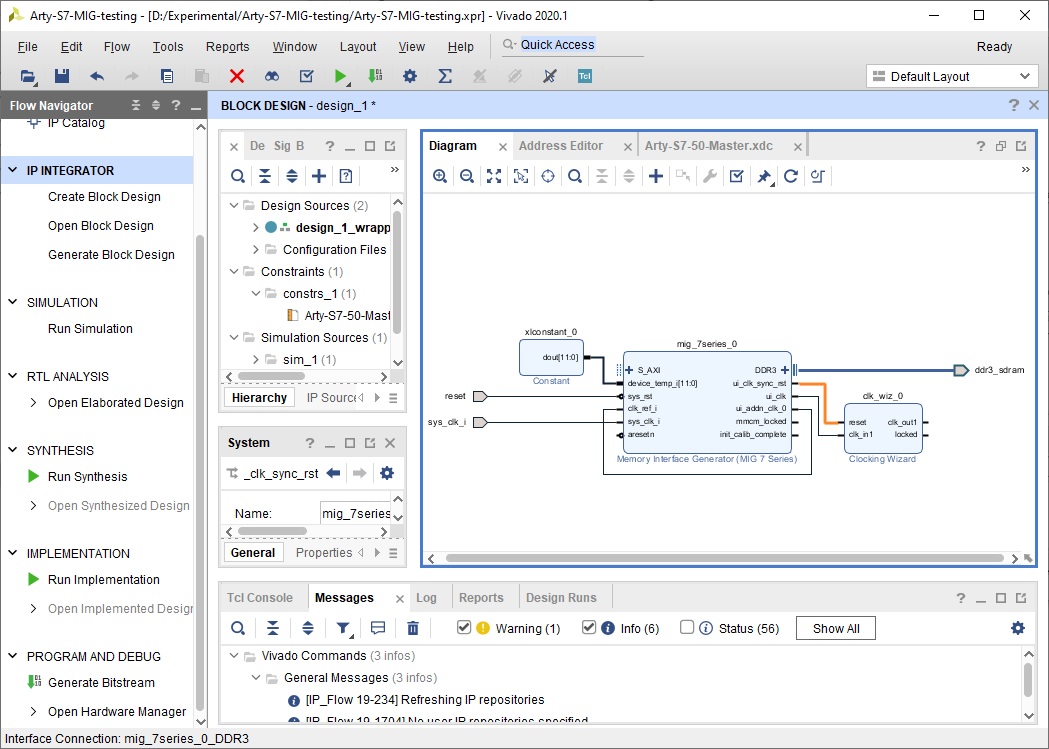
Finally, double-click on the Clocking Wizard to open and configure it. The third tab, Output Clocks contains all of the settings required to specify how many clocks you need, and of what frequencies. The screenshot to the right shows the wizard configured to create a 100 MHz clk_out1 and a 50 MHz clk_out2.
If your design requires additional clocks (such as for an ext_spi_clock pin), they should be added here.

Note: If you aren't sure that you have all of the clocks you need, don't worry, you can always come back and add them by reconfiguring this IP. This task can be performed whenever in the design process it becomes necessary.
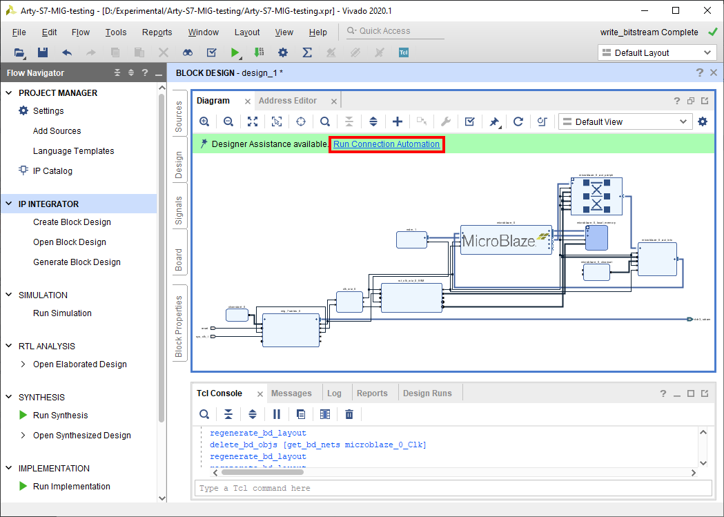
At the end of this process, the block design will look something like this:
Next, use the Add IP button (
) to add the MicroBlaze IP to the design. The block that is added represents the core of the Microblaze processor.
Next, block automation will be run so that additional supporting infrastructure can be added to the design. Click Run Block Automation in the green Designer Assistance bar.
Note: The screenshot to the right is not representative for a design not using DDR, as these designs will not contain a MIG IP core.
In the Run Block Automation dialog, several settings can be specified for how the Microblaze IP will be connected to the rest of the design:
- Local Memory specifies how much block RAM memory will be dedicated to the processor. DDR-less designs require more memory, and the amount of memory necessary depends heavily on the size of the software application being run. 32KB is enough for many small applications.
- Cache Configuration can help the speed of designs using DDR memory. It should be enabled when using DDR, and disabled otherwise.
- Debug Module allows you to specify the capabilities of the debugger. The default Debug Only option is recommended.
- Peripheral AXI Port enables or disables the AXI master interface of the processor. It must be enabled to allow the processor to be connected to hardware peripherals.
- Interrupt Controller specifies whether the processor can be interrupted by its peripherals. Whether or not it needs to be enabled depends on your design requirements. If any IP that you intend to connect to the processor must have interrupts to function correctly, the box must be checked.
- Clock Connection specifies the processor's clock. Designs using DDR should use the MIG's ui_clk pin, while designs without DDR should use the Clocking Wizards clk_out1 pin.
Note: Settings not present in this list are out of the scope of this guide, and can safely be left as their default.
Confirm that the settings meet your design requirements. It should be noted that while it is possible to change these settings manually later (for example, by manually adding an AXI INTC IP and connecting it to the processor), the easiest way to do so will be to clear the Microblaze processor out of your block design and restart the process of adding the processor. This is to say, the settings chosen here are important. Getting them right the first time will save you time in the long run.
Important! When working with multiple clocks in a design (as happens to always be the case when working with the MIG) it is important to verify that you are picking the correct Clock Connection from the dropdown. In the screenshot to the right, the 100 MHz clk_out1 from a clocking wizard is chosen. You may instead wish to run your design off of ui_clk itself. Do not select the system clock input to the MIG.
Click OK to continue.
Next, the MIG's AXI interface must be connected to Microblaze's cache ports, in order to allow data to move back and forth between processor and DDR memory.
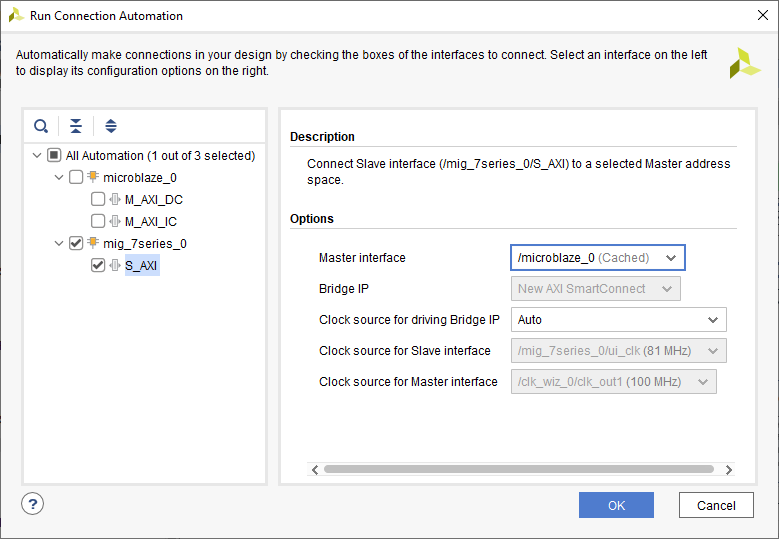
To connect the MIG's AXI interface to the processor, click the Run Connection Automation button in the green banner at the top of the block design.
In the dialog that pops up, you will be presented with several options for interfaces that can be connected to other interfaces. Both the Microblaze's IC and DC ports, as well as the MIG's AXI port will appear. You should only run connection automation for one side of the connection - the S_AXI port, as shown in the screenshot to the right. Make sure that its box is checked. Check that the Master interface is set to “/microblaze_0 (Cached)”, indicating that the microblaze local memory will act as a cache for the DDR memory, then click OK to make the connections.
Next, in order for the software design to be able to print to a serial console on a host computer, a UART peripheral must be connected. Find the USB UART interface in the Board tab, right click on it, and select Connect Board Component.
In the dialog that pops up, select a new AXI Uartlite IP's UART interface, and click OK to add the block to the diagram.
To connect all remaining AXI cores that have not yet been connected to the processor, click the Run Connection Automation button in the green Designer Assistance bar. Check the All Automation box in the list on the left side of the window to select all of the remaining AXI cores. The dropdown settings available for each core can safely be left as their default values. Click OK to automatically connect them to the processor.


- Add a Zynq Processor to a Block Design
-
The Zynq7 Processing System IP represents the non-FPGA components of a Zynq chip, referred to as the Processing System, or PS. It must be used in a block design that wants to connect anything to the processor, and to configure PS-side peripherals, clocks, and other settings.
Note: This section only applies to boards with a 7-series Zynq chip.
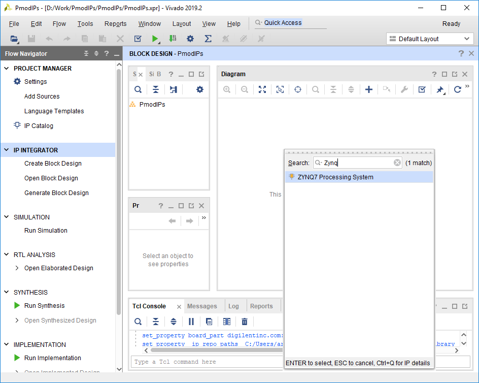
In the block diagram pane's toolbar, click the Add IP button (
).
In the pop up, search for and double click on ZYNQ7 Processing System.
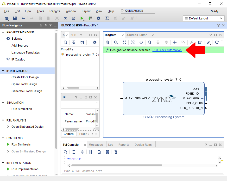
Click Run Block Automation in the Design Assistance banner (the green bar).
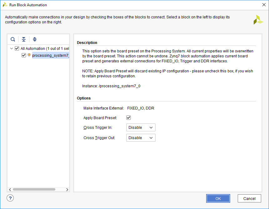
In the dialog that pops up, leave all settings as defaults. Apply Board Preset should be checked.
The needs of your project may require that you change some of the default settings of the Zynq PS. To edit its settings, double click on it to open the configuration wizard.
Two specific cases are highlighted below:
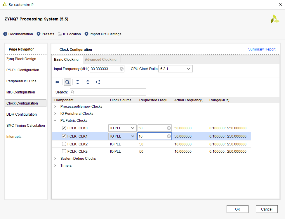
The Zynq PS can generate multiple clocks that are then provided to the FPGA fabric. These clocks are referred to as FCLKs, and can be found in the Clock Configuration tab of the Zynq PS configuration wizard. They are located under the PL Fabric Clocks dropdown. They can be enabled (or disabled) with a checkbox, the hardware used to drive the clock can be changed, and the frequency can be modified.
All board files for Digilent Zynq boards enable a single Zynq PL clock by default, which is intended to be used with peripherals connected to the Zynq's M_AXI_GP0 port.
Some designs may require additional clocks of specific frequencies be added to your design. In these cases, enable a second clock and specify the needed frequency, as seen in the image to the right.
Note: This section can always be returned to later, as the addition of an additional clock can be performed any time before the hardware is built.
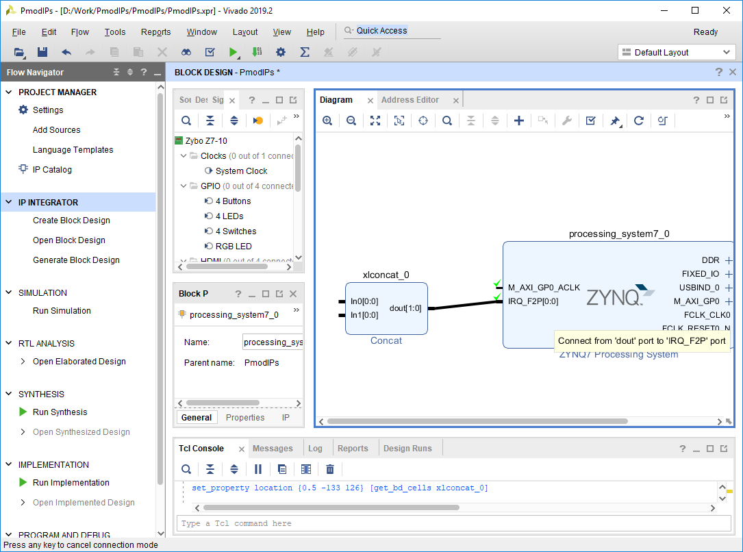
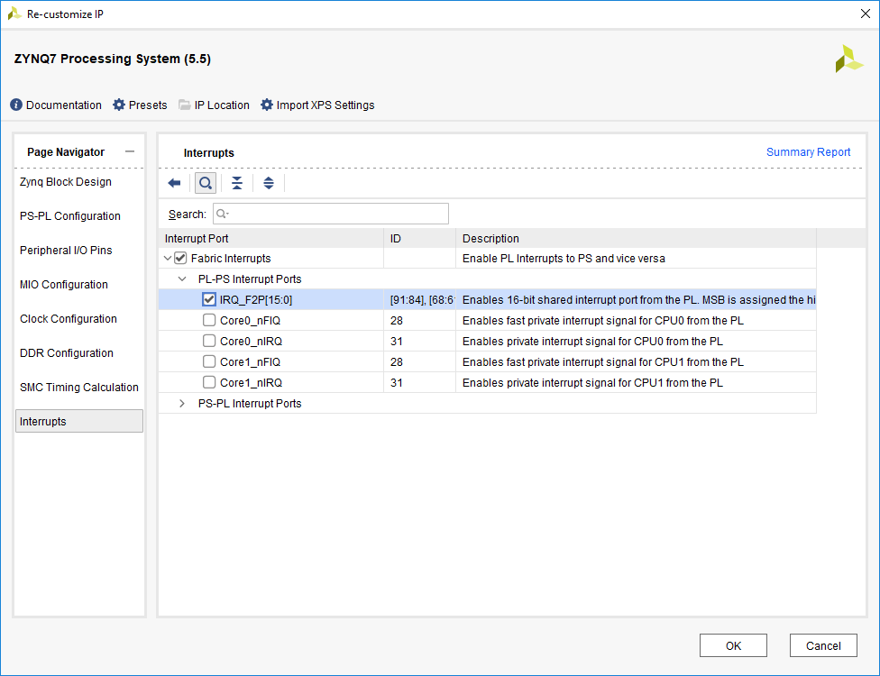
Zynq devices can also use interrupts generated in FPGA fabric to trigger interrupts within the Processing System. Interrupt-related settings can be changed within the configuration wizard's interrupts tab. These interrupts typically use the IRQ_F2P port, which can be found under the Fabric Interrupts → IRQ_F2P dropdown. To enable this port, both the Fabric Interrupts and IRQ_F2P ports must be enabled.
While interrupts can be directly connected to the IRQ_F2P port (by clicking and dragging from one port to another), some designs may require multiple interrupt sources. In these cases, add a Concat IP to your block design, and manually connect it to the IRQ_F2P port. Additional input ports can be added to a Concat block through its configuration wizard (opened by double clicking on the IP).