Add GPIO Peripherals to a Block Design
This section covers the steps involved in adding a GPIO peripheral to a block design. While an AXI GPIO IP is used, other IPs and interfaces can potentially be added to your design in the same ways. Two methods are presented here, one for each of the two AXI GPIO peripherals that will be connected. The first takes advantage of board files to automatically generate constraints, the second presents how an IP interface can be connected to chosen pins manually.
Interfaces for Digilent boards supported by the board files can be found in the Board tab. For the purposes of this guide, find the GPIO section of the list, right click on an LED interface, and select the Connect Board Interface option.
Note: If your board does not have single-color LEDs, you can use it's RGB LEDs instead. Note that these interfaces have three pins for each LED, for the R, G, and B components.

In the dialog that pops up, choose the “GPIO” interface (not GPIO2) of a new AXI GPIO IP.
Some boards use one of their user buttons as reset sources. In these cases, make sure to choose the Component mode that does not include the reset button.
Click OK to continue. This will add the IP to your design, and connect it to an external port, which will not require any further work to constrain.

Next, select the axi_gpio_0 block. The Block Properties pane to the left of the Diagram and below the Board tab will allow you to view some information about the block, and modify it in some ways, without running through its customization wizard. For now, just change its name to “AXI_GPIO_LED” by typing in the Name field. Pressing enter or clicking out of the text box confirms the change. Using memorable names in your block design makes it easier to remember which IP does what when you are later writing software in Vitis.

Next, a second AXI GPIO IP will be manually added to the block diagram, and manually constrained with an XDC file. Click the Add IP button ( ) and search for “AXI GPIO”. Double click on the only result to add the second AXI GPIO block to the design. Once added, rename this IP “AXI_GPIO_BUTTONS”

Select the AXI_GPIO_BUTTONS IP's GPIO interface by clicking on the text “GPIO”, right click on the highlighted text, and select Make External. This option creates a new external interface port that does not rely on the board files. Because the board files are not used here, a Xilinx Design Constraint (XDC) file must be added to the project to tell Vivado which FPGA pins to connect the interface to.

If your project doesn't contain the master Xilinx Design Constraint (XDC) file for your board, the dropdown below details how to add it. This file contains the constraints that your board places on designs using it - specific interfaces wired up to specific pins, clock frequencies, and FPGA bank voltages, for some examples. Click the dropdown below for a walkthrough of how to add this file to your project.
- Add a Master XDC File to a Vivado Project
-
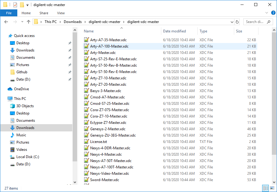
Download and extract digilent-xdc-master.zip. This file includes all of the latest template XDC files released for Digilent's boards, which are available on Github in the digilent-xdc repository.
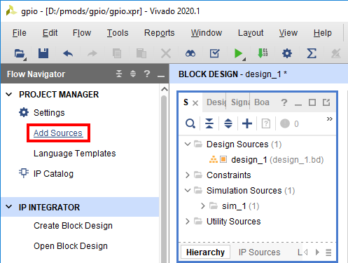
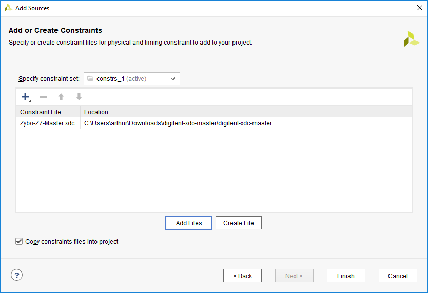
Returning to Vivado, click the Add Sources button in the Project Manager section of the Flow Navigator pane. This will launch a dialog that you can use to add a variety of types of source files to the project (or create new ones).
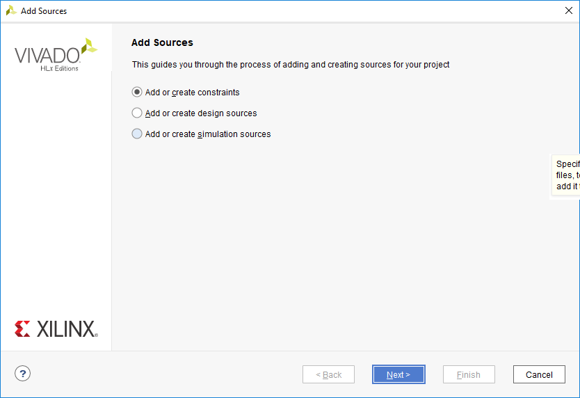
On the first screen, select Add or create constraints. Click Next to continue.
In the next screen, make sure that the constraint set specified (the one that the master XDC will be added to) is set to constrs_1, and that it is the active set. Click the Add Files button.

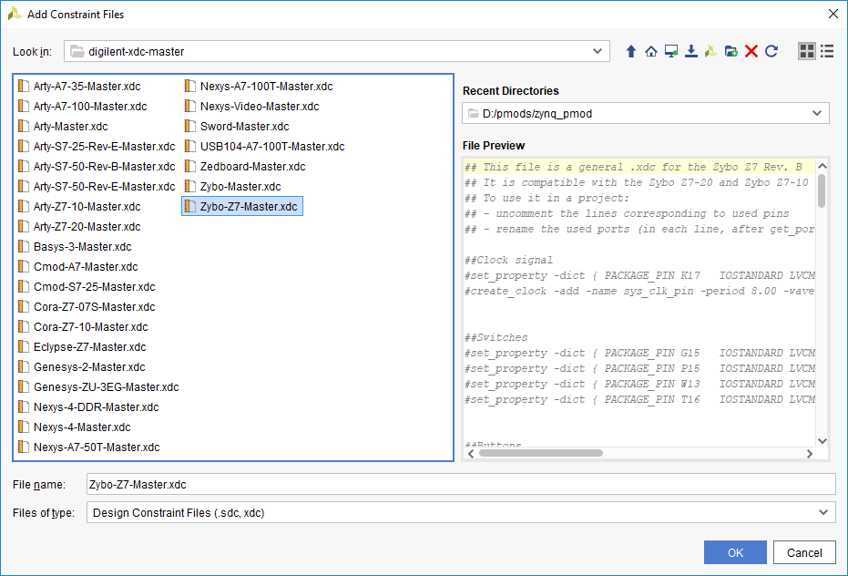
In the dialog that pops up, navigate to the folder that the digilent-xdc-master.zip file was extracted into. Highlight the XDC file for your board, then click OK to continue.
Back in the Add Sources dialog, make sure that your chosen constraint file appears in the table. Also, make sure that the Copy constraint files into project box is checked. If this box is unchecked, the file will be linked by your project, and any modifications made within the project will affect the version you downloaded. Since you may need to use this file again in other projects, copying the constraint file is recommended, so that you can always work from a fresh copy.
Click Finish to add the constraint file to your project.
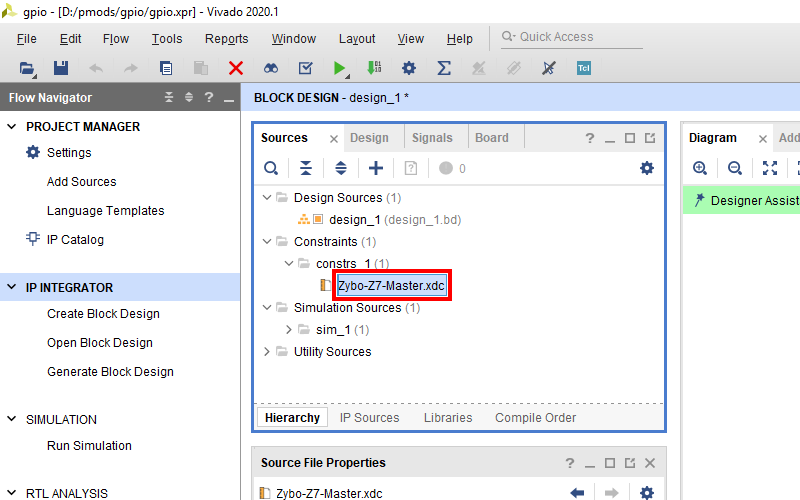
Once added, the XDC file will appear in the Sources tab (in the same pane as the Board tab). Double click it to open the file.


Master XDC files for Digilent boards contain pin constraints for I/O interfaces the board offers. These constraints are sorted by interface. Scroll down until you see constraints for the user buttons. These constraints typically are for a bus port named “btn”. Un-comment the button constraints by removing the single leading '#' character in each line corresponding to the buttons, as seen in the screenshot to the right.

Next, the names of the block design's GPIO port for the buttons must be determined, so that the buttons can be properly constrained. Reopen the Diagram tab, and select the GPIO_0 external port that is connected to the AXI_GPIO_BUTTONS block. Change the name of the external interface to “btn” in the Properties pane.
The AXI GPIO IP automatically uses tri-state buffers for the pins its interfaces are connected to. The individual I, O, and T buses can be seen when expanding the interface through the plus button ( ) next to the interface name on the IP block. As can be seen, the individual ports that make up the interface are named <interface>_tri_i, <interface>_tri_o, and <interface>_tri_t. When constrained to tristate buffers, the bus that is connected to FPGA ports is named <interface>_tri_io.

With this knowledge, return to the XDC file, and change the name of the button bus that is constrained. Specifically, change the text after the “get_ports” call on each line of the button interface to “btn_tri_io[#]”, where # is a decimal number, counting up from zero. When finished, save the file.
With the constraints for the port finished, the AXI GPIO must be manually configured. In particular, the width of the GPIO interface must match the number of buttons available on the board. Take note of how many buttons are constrained in the XDC.

Return to the Diagram tab, and double click on the AXI_GPIO_BUTTONS block. This will open a dialog that will allow you to configure the IP's settings. Switch to the configuration wizard's IP Configuration tab.
Only one setting need be changed for the purposes of this guide. Enter the number of buttons you constrained into the GPIO interface's GPIO Width field. When finished, click OK to save your changes.

Finally, the two AXI GPIO IP blocks need to be connected to the processor in your design. Click the Run Connection Automation button in the green Designer Assistance bar.

In the dialog that pops up, make sure that the boxes for the S_AXI interfaces for both of the AXI GPIO IPs are checked. Click OK to run connection automation and connect the AXI GPIO blocks to your processor.
