This is an old revision of the document!
simulation
UNDER CONSTRUCTION
Learning digital logic design, Verilog and FPGA programming can be quite overwhelming at first, so much so that taking on another topic, such as simulation, is avoided. However, it well worth it to see how well your Verilog design will respond to external stimulus and in the process perhaps provide you with a better understanding of how Verilog code responds. So what is Simulation?
A simulation module, also known as a test-bench, produces fake signals used to see how a design module responds. The simulation environment itself is able to provide nanosecond timing and is much more than setting values to ones or zeroes. And, because the test code does not have to be synthesizable, we can use additional constructs provided by SystemVerilog that make it easier to generate test elaborate test conditions.
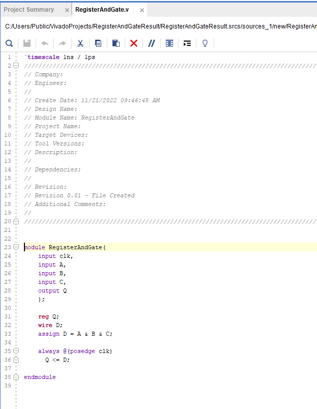
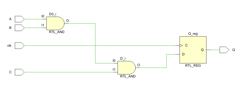
In the following example, we will use Vivado 2022.1 Simulation to see how a design behaves to inputs. The design consists of a three input AND gate and a D-Flip-Flop to register the output. We will also take a look at a module designed to debounce mechanical switch closures and provide a slightly different approach to simulation.
We will start with the first design and its RTL Schematic diagram
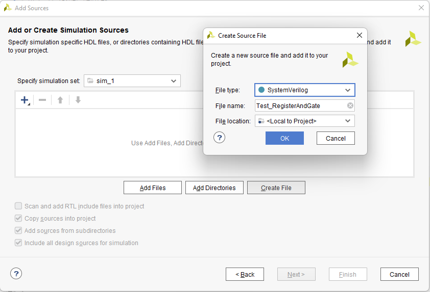
To begin, we need to add a simulation source file to our project. If you require a review of creating a simple design project, see Getting Started with Vivado for Hardware-Only Designs. Under the Project Manager section, choose Add Sources and create a simulation source file.
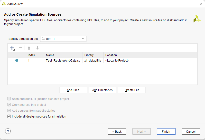
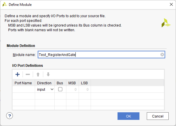
We want to create a SystemVerilog file instead of Verilog file. A SystemVerilog file exposes additional constructs that can be very helpful with our simulations. Give the simulation file a name. Our design module is called RegisterAndGate, so we will use Test_RegisterAndGate to indicate it is a simulation module. Press OK followed by Finish.
Before completing the process, the wizard will ask if our simulation module uses inputs and outputs. In general, test-bench modules do not use inputs or output, so press OK to continue followed by YES for confirmation.
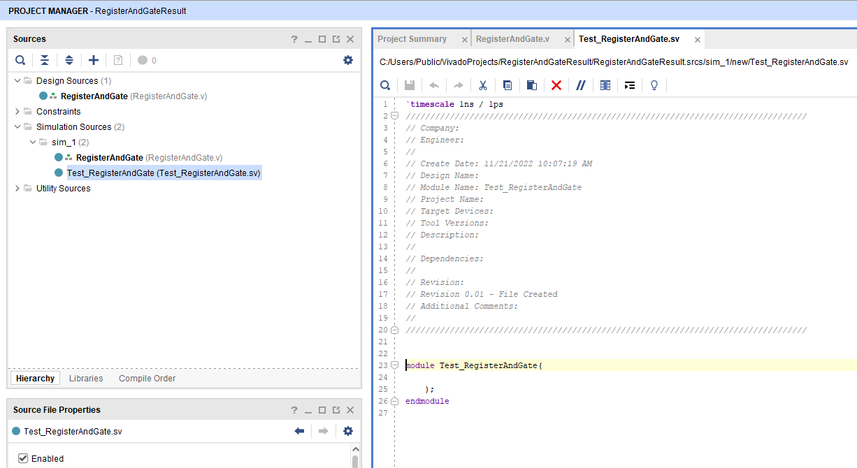
Double-click the new file shown under Simulation Sources→sim_1 and Vivado will generate and display the file
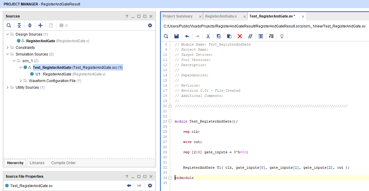
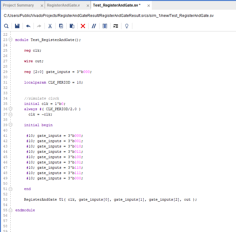
For test purposes, inputs to the module to be tested are registers and its outputs are wires. For the three inputs add one three bit register, for the one output add a wire. Instantiate the design module as U1 (or any name of your choosing) as shown below and save the file.
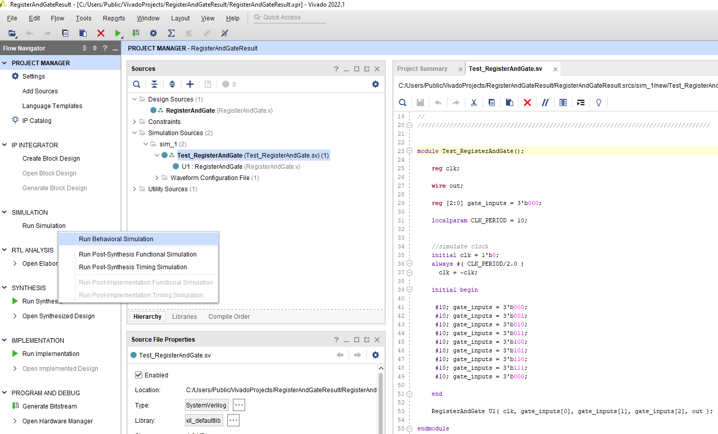
Notice that under Simulation Sources→sim_1, the test module now appears as a child to the simulation module.
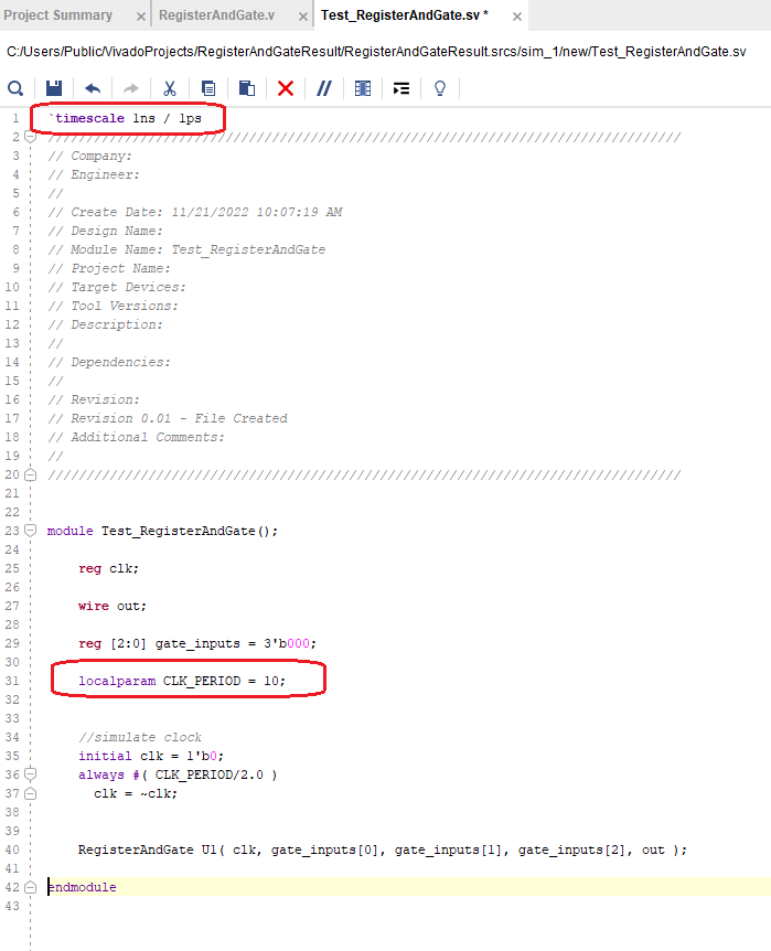
Next, the design uses a flip-flop to register the AND gate output, so we need to create a clock. Add a local parameter CLK_PERIOD = 10 to designate the clock period. 10 indicates 10nS denoted by the `timescale 1ns / 1ps line at the top.
Initial clk = 1’b0;
Always # (CLK_PERIOD / 2.0)
clk = ~clk;
Edit Test_RegisterAndGate.sv as shown below. This code will generate a continuous clock that has a 10nS period. Save the file before continuing.
Now, we need the individual test steps. For this, we will use the brute-force method of individual setting each condition and time duration. See the initial begin block below. The #10 is a 10nS delay. Each line is a variation of the three AND gate signals along with a time delay. #10 just happens to be the period of the clock, but it is an arbitrary number. You could use #2, #3, #5 and so on however, if the delay is shorter than the clock period, the result may not be registered to the output. Save the file and continue.
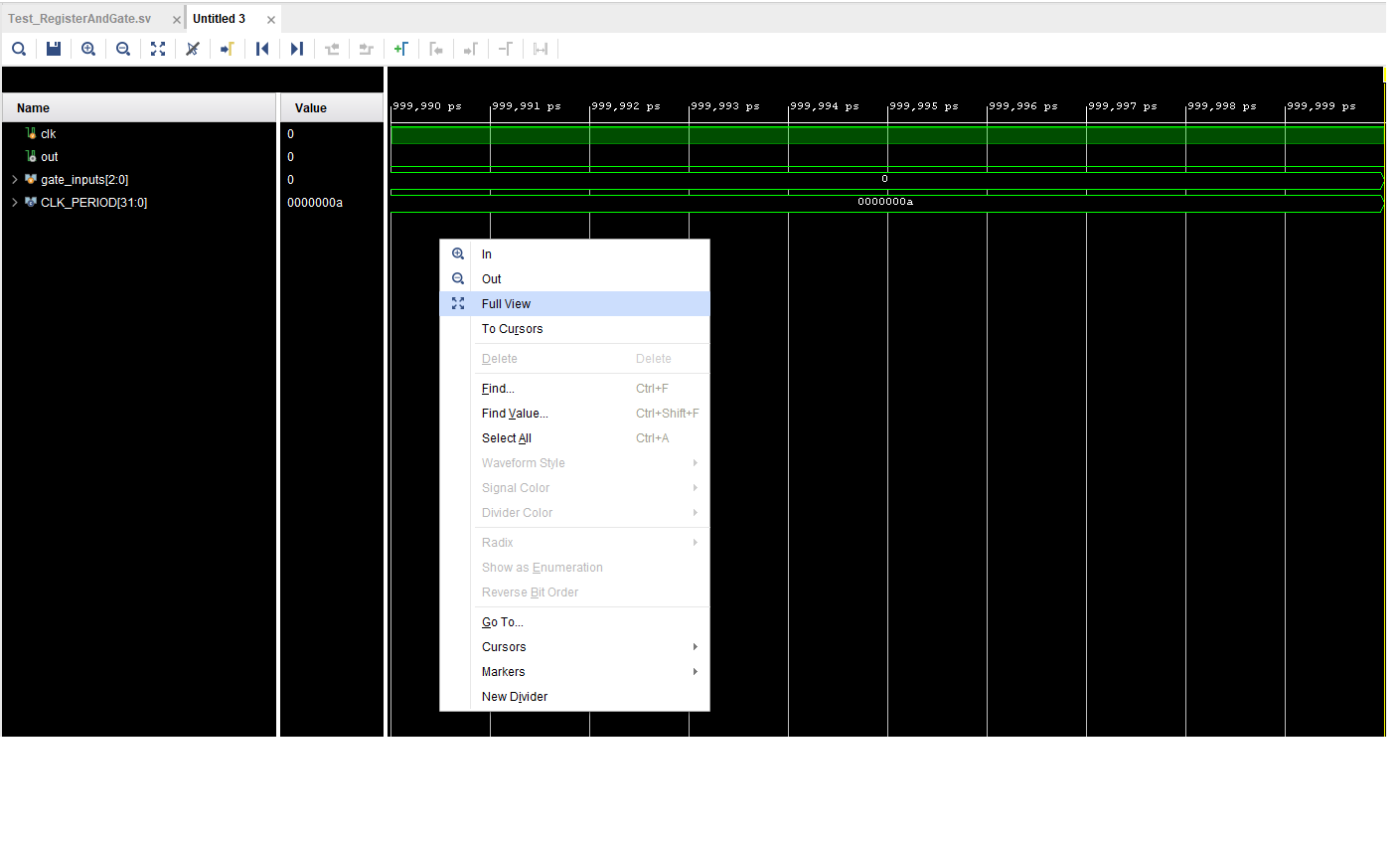
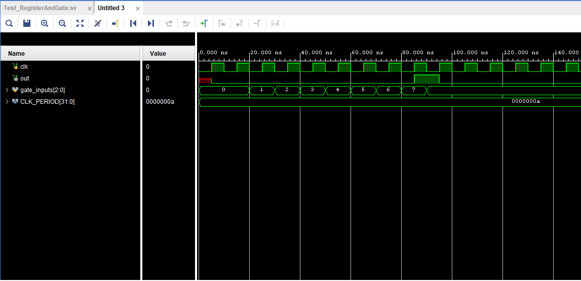
After the simulation has run, the Wave-Window should open displaying the results graphically. The default time for a simulation is 1000nS. This time can be adjusted via the Simulation Settings. To get a better picture of our signals, select Full View and zoom in. To select Full View, right-mouse click the screen and choose Full View.
Hit the (+) magnifying glass icon twice then move the x-axis slider to the beginning (left) to see the simulation.
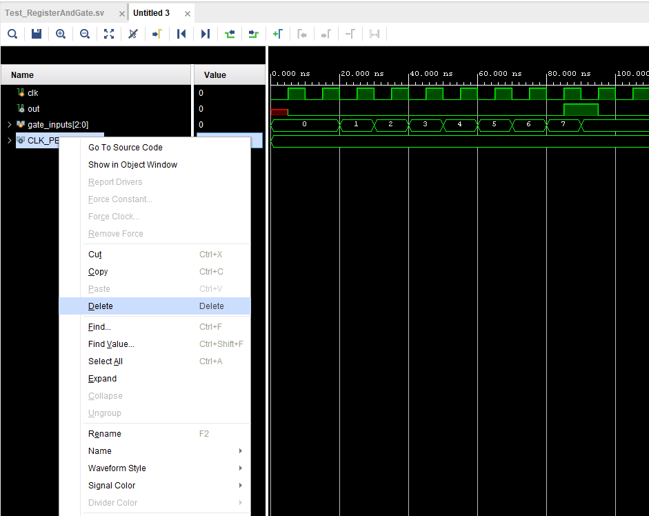
A signal can be deleted from the Wave-Window by first selecting it, followed by a right-click-Delete. Or select it and press the Delete key.
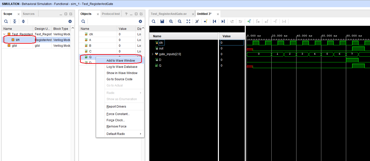
Signals can also be added. For instance, choose U1 (instantiated design module) in the Scope tab. This will list the signals inside U1, right-mouse click and choose Add to Wave-Window.
From the previous Wave-window results, the gate_inputs register counts from zero to seven testing the eight combinations of the inputs. When the gate_inputs register equals seven, or all three inputs are high, the output of the AND gate is high and on the next clock edge after, the flip-flop output Q is set high, indicating correct behavior.
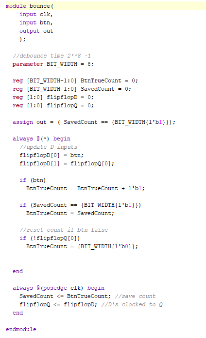
Next, if the AND gate inputs are to be used to sense mechanical switches, a debounce circuit should be used. Below is a simple debounce algorithm. It works by detecting a switch closure that starts an incrementing counter. It will count up to a maximum value, at which time it is assumed that the input signal is stable. If the switch closure is not perfect and it bounces up and down (also known as jitter or chatter), the count is forced to start over. This keeps happening until it is stable enough to let the count reach the maximum value. To lengthen the debounce period, make the register width wider so it counts to a larger number. The following is the debounce algorithm. Design inspired by the Metastability and Debouncing Verilog blog from Alchitry.com
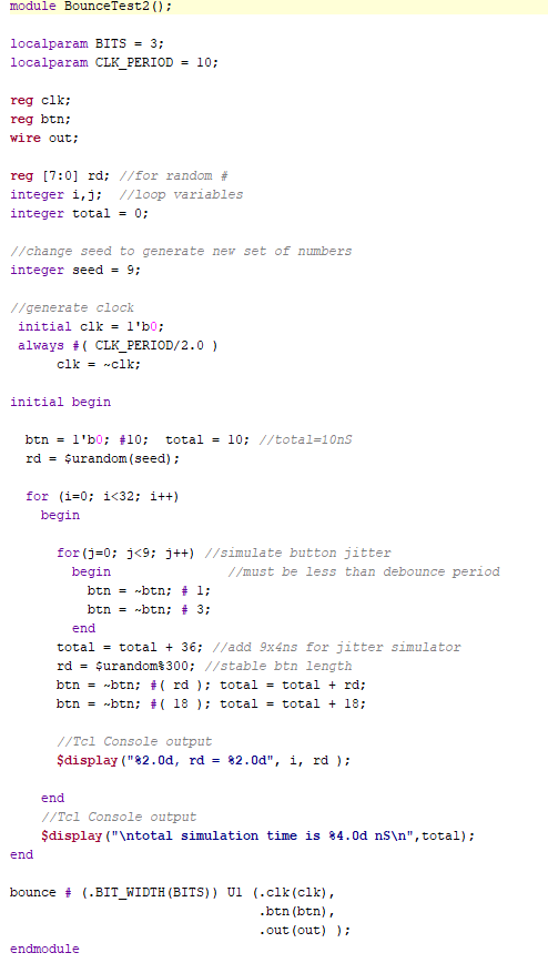
The following is its test-bench file. For simplicity, it overrides the default register width of eight and instead uses three bits for a maximum count of seven. Instead of using single step set and wait statements to test the module, we can use For loops to generate the signals. We can also take advantage of additional constructs the SystemVerilog file offers and use the $random function to generate the time that a signal will be true. Note, in order to generate different numbers each time the simulation is run, the seed number must be changed.
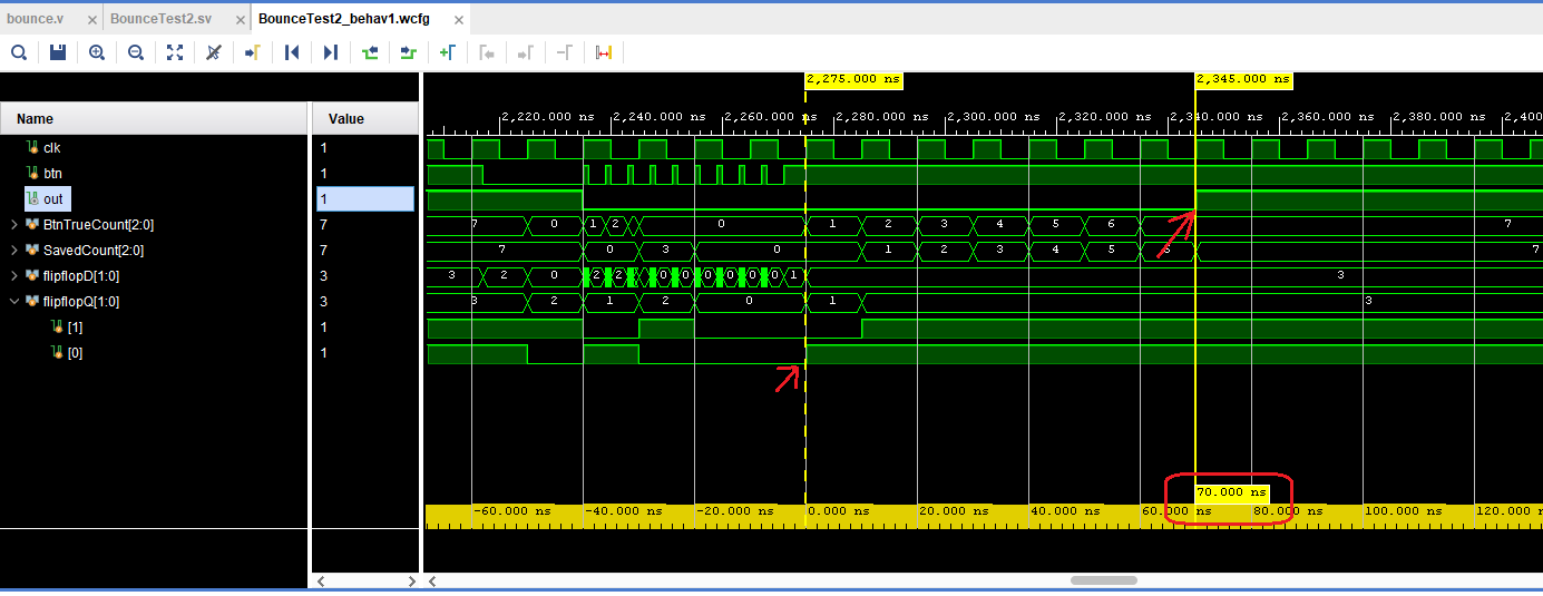
BounceTest2 uses nested For loops. The inner For loop simulates the switch closure jitter and the outer loop simulates the non-jitter or stable period of the closure.
In the simulation output below, we can see the rapid fire of the simulated switch jitter as it makes contact. We can also see when SavedCount begins to count, when it reaches seven and when the output is set and when it is released
We can measure the time from when the button is registered by the first flip-flop (count begins) to when the bounce.v module sets the output high. Use the mouse and click the Wave at the start point to set the cursor. Hold down the shift key and click the Wave at the stop point and it will calculate the elapsed time. Here we see that our three bit register provides 70nS of debounce. For a practical application, this is much too short. Consider times that are greater than 1uS (7 bit register)..
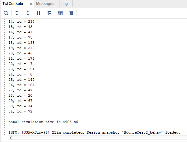
Our test-bench can also output values to Tcl console. To do this we use the $display function, which is like the printf C-code function. In this example, the duration for individual test signals is displayed as well as the total simulation time at the end.

