Using the Simulator in Vivado
Learning digital logic design, Verilog, and FPGA programming can be quite overwhelming at first, so much so that taking on another topic, such as simulation, is often avoided by newcomers. However, it's well worth it to see how well your Verilog design will respond to external stimuli and in the process perhaps provide you with a better understanding of how Verilog code responds. Plus, if and when you start running into problems with figuring out why your design isn't working as intended, simulation provides a relatively easy way to approach debugging it. So, what is Simulation?
A simulation module, also known as a test-bench, produces fake signals used to stimulate a design module and see how it responds. The simulation environment itself is able to provide nanosecond timing and is much more than just setting values to ones or zeroes. And, because the test code does not have to be synthesizable, we can use additional constructs provided by SystemVerilog that make it easier to generate elaborate test conditions.
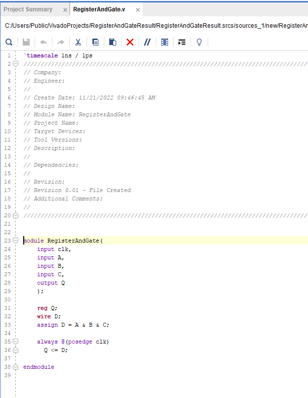
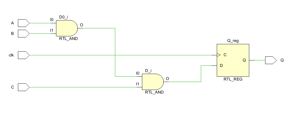
In this guide, we will use Vivado's built-in Simulator to see how a design behaves as its inputs change. The first design under test consists of a three-input AND gate and a D-Flip-Flop to register the output. We will also take a look at a module designed to debounce mechanical switch closures and provide a slightly different approach to simulation.
Inventory
- All you need to follow this guide is a Vivado installation.
- This guide was written using Vivado 2022.1, however other versions will work largely the same, with some minor visual differences.
- If you haven't already, check out Installing Vivado, Vitis, and Digilent Board Files for instructions on how to install Vivado
Guide
This guide contains two examples:
- Simulating a Simple D-Flip-Flop presents how to get your first simulation going in Vivado
- Simulating a Debouncer presents several useful features of the simulator, including measuring time from one event to another and using random values to generate a test waveform.
Simple D-Flip-Flop Example
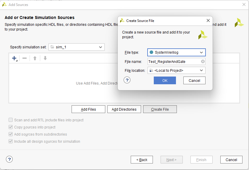
To begin, we need to add a simulation source file to our project. If you require a review of creating a simple design project, see Getting Started with Vivado for Hardware-Only Designs. Under the Project Manager section, choose Add Sources and create a simulation source file.
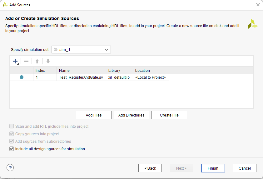
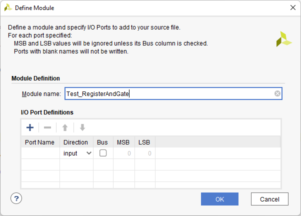
We want to create a SystemVerilog file instead of Verilog file. A SystemVerilog file exposes additional constructs that can be very helpful with our simulations. Give the simulation file a name. Our design module is called RegisterAndGate, so we will use Test_RegisterAndGate to indicate it is a simulation module. Press OK followed by Finish.
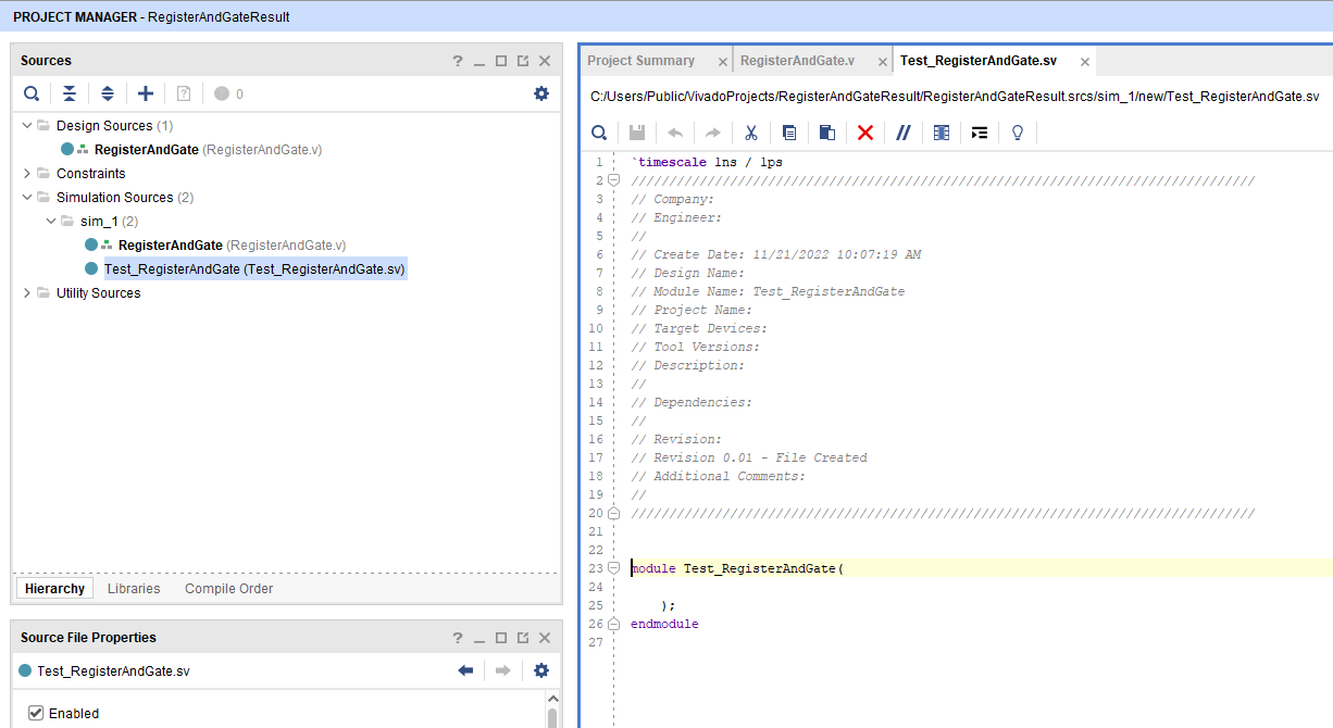
Before completing the process, the wizard will ask if our simulation module uses inputs and outputs. In general, top-level test-bench modules do not use inputs or output, so press OK to continue followed by YES for confirmation.
Double-click the new file shown under Simulation Sources→sim_1 and Vivado will generate and display the file.
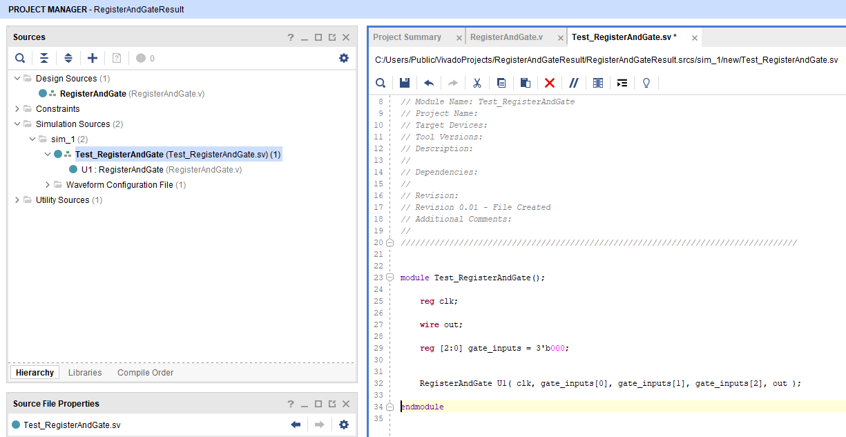
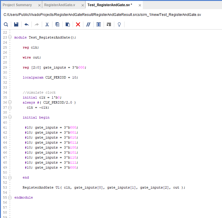
For test purposes, inputs to the module to be tested are registers and its outputs are wires. For the three inputs add one three-bit register. For the one output add a wire. Instantiate the design module as U1 (or any name of your choosing) as shown below and save the file.
Notice that under Simulation Sources→sim_1, the test module now appears as a child of the simulation module.
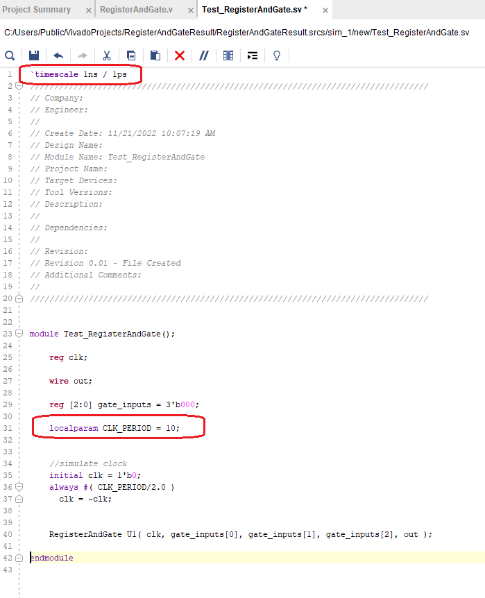
Next, the design uses a flip-flop to register the AND gate output, so we need to create a clock. Add a local parameter named CLK_PERIOD with a value of 10 to designate the clock period. 10 indicates 10 nS denoted by the `timescale 1ns / 1ps line at the top.
The following chunk of code initializes the clock to logic zero and toggles (inverts) it every 5 ns for as long as the simulation is running:
initial clk = 1’b0;
always #(CLK_PERIOD / 2.0)
  clk = ~clk;
Edit Test_RegisterAndGate.sv as shown to the right. This code will generate a continuous clock that has a 10 nS period. Save the file before continuing.
Now, we need the individual test steps. For this, we will use the brute-force method of individually setting each condition and time duration. See the initial-begin block below. The #10 is a 10 nS delay. Each line is a variation of the three AND gate signals along with a time delay. #10 just happens to be the period of the clock, but it is an arbitrary number. You could use #2, #3, #5, and so on, however, if the delay is shorter than the clock period, the result may not be registered to the output. Save the file and continue.
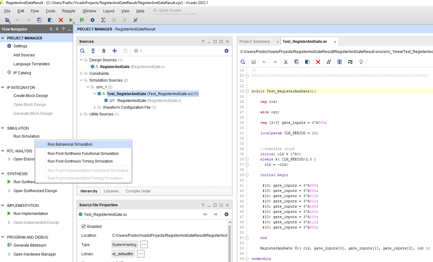
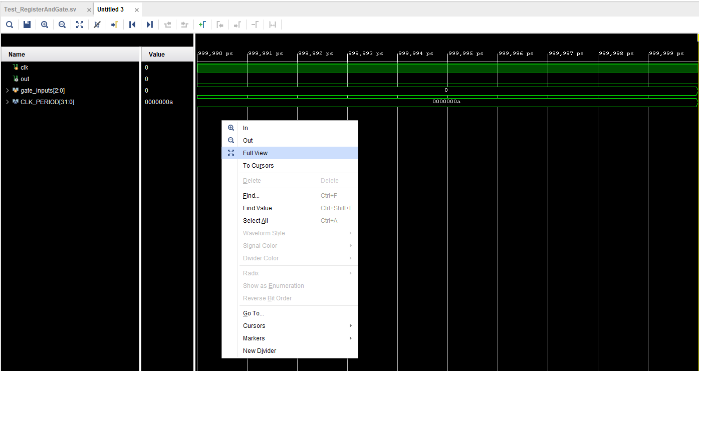
After the simulation has run, the Wave-Window should open displaying the results graphically. The default period for a simulation is 1000 nS. This time can be adjusted via the Simulation Settings. To get a better picture of our signals, select Full View and zoom in. To select Full View, right-mouse click the screen and choose Full View.
Hit the (+) magnifying glass icon twice then move the x-axis slider to the beginning (left) to zoom in on the main region of interest.
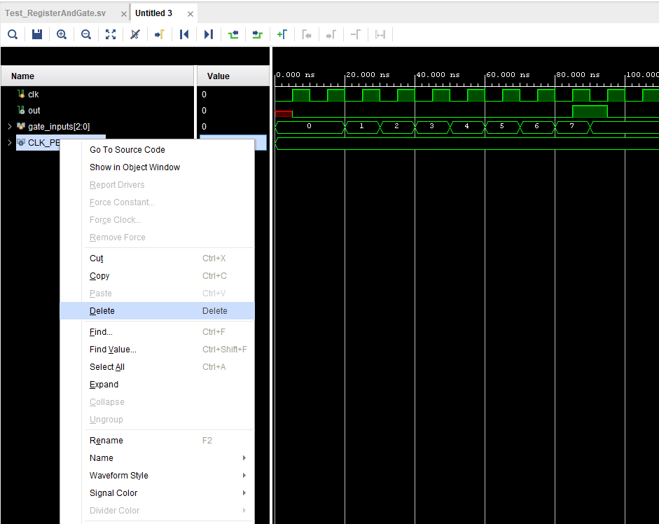
We already know what the CLK_PERIOD is, so we don't want it cluttering up the screen. If we were taking a look at a more complex design with many more signals it would be taking up prime real estate. Go ahead and delete its trace:
A signal can be deleted from the Wave-Window by first selecting it, followed by a right-click-Delete. Or select it and press the Delete key.
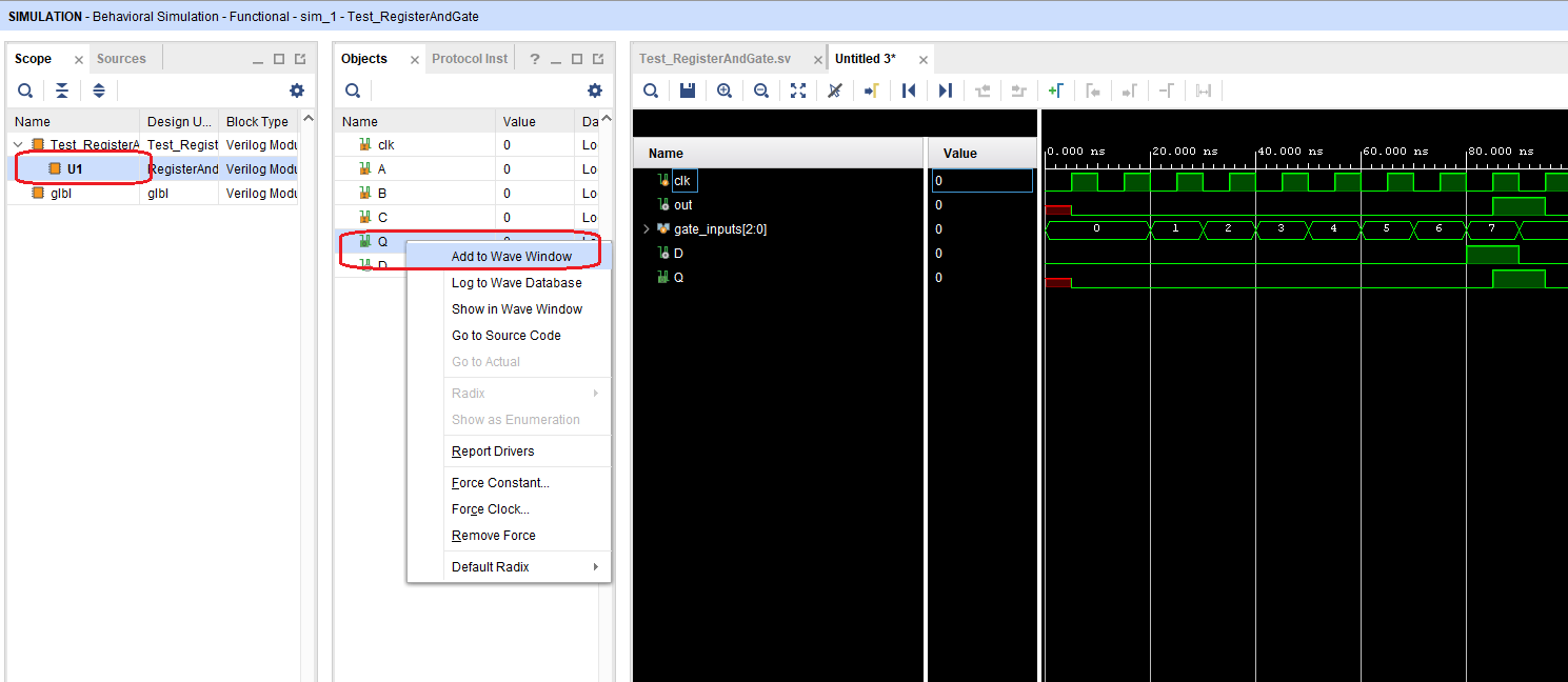
Internal signals can also be added from within the instantiated module. For instance, choose U1 (the instantiated design module) in the Scope tab. This will list the signals inside U1, right-mouse click and choose Add to Wave-Window.
These signals typically start out without recorded waves when first added to the window, so you may need to either relaunch the simulation or reset it and run it forward again in order to get these signals to appear.
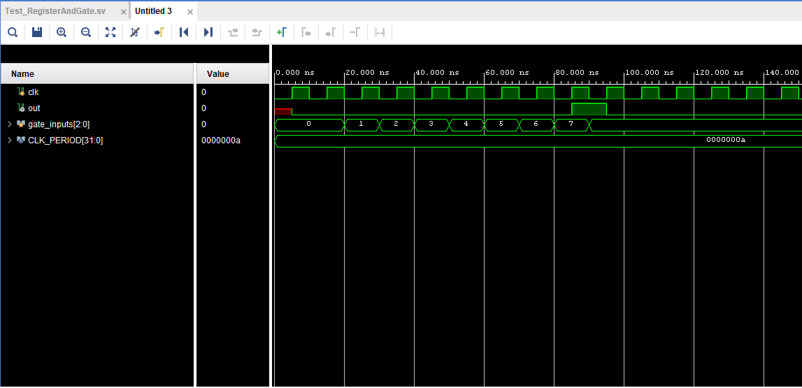
From the previous Wave-window results, the gate_inputs register counts from zero to seven testing the eight combinations of the inputs. When the gate_inputs register equals seven, or all three inputs are high, the output of the AND gate is high and, on the next clock edge after, the flip-flop output Q is set high, indicating correct behavior.
Debouncer Example
A debouncer is a common circuit used in many applications to ensure that noise is removed from slow incoming signals. If the AND-gate circuit above were directly connected to buttons, the output signal might include noisy glitches whenever a button is pressed, due to the noisy nature of how the mechanical switch closes. Adding a debouncer to each incoming signal would remove this noise.
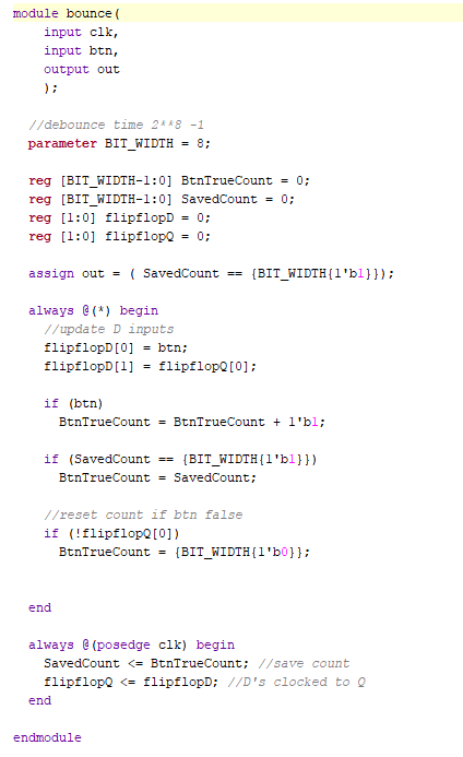
The code to the right implements a simple debounce algorithm1). It works by starting an incrementing counter whenever a switch closure is detected. It will count up to a maximum value, at which time it is assumed that the input signal is stable. If the switch closure is not perfect and it bounces up and down (also known as jitter or chatter), the count is forced to start over. This keeps happening until it is stable enough to let the count reach the maximum value. To lengthen the debounce period, make the register width wider so it counts to a larger number.
The following is the debounce algorithm.
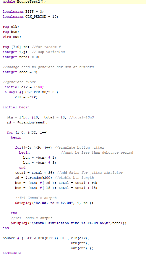
The following is its test-bench file. For simplicity, it overrides the default register width of eight and instead uses three bits for a maximum count of seven. Instead of using single-step set and wait statements to test the module, as we did for the AND gate, we can use For loops to generate the signals. We can also take advantage of additional constructs the SystemVerilog file offers and use the $random function to generate the time that a signal will be true. Note, in order to generate different numbers each time the simulation is run, the seed number must be changed.
BounceTest2 uses nested For loops. The inner For loop simulates the switch closure jitter and the outer loop simulates the non-jitter or stable period of the closure.
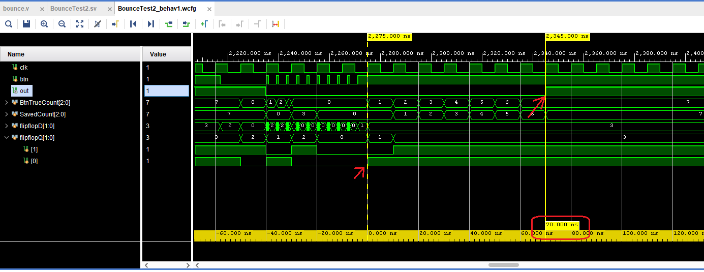
In the simulation output below, we can see the rapid fire of the simulated switch jitter as it makes contact. We can also see when SavedCount begins to count, when it reaches seven, and when the output is set and when it is released.
We can measure the time from when the button is registered by the first flip-flop (count begins) to when the bounce.v module sets the output high. Use the mouse and click the Wave at the start point to set the cursor. Hold down the shift key and click the Wave at the stop point and it will calculate the elapsed time. Here we see that our three-bit register provides 70 nS of debounce. For a practical application, this is much too short. Consider times that are greater than 1 uS (7-bit register).
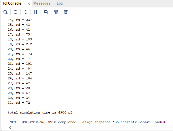
Our test-bench can also output values to the Tcl console. To do this we use the $display function, which is like the printf C-code function. In this example, the duration for individual test signals is displayed as well as the total simulation time at the end.
Final Notes
For more guides on using Digilent FPGA boards with Vivado, check out their resource centers, which can be found through the Programmable Logic landing page.
For technical support, please visit the Digilent Forums.

