Advanced Microblaze Design using Memory Interface Generator (MIG), Ethernet, UART & GPIOs
!*!*UNDER CONSTRUCTION*!*!
This page is currently under development and may not be a complete demo at this time. This notice will be removed once the tutorial is in a stable state
Description
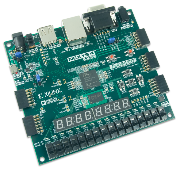
This guide will provide a step by step walk-through of creating a Microblaze based hardware design using the Vivado IP Integrator that will build over the [nexys4-ddr:gsmb|Getting Started with Microblaze]] guide by making use of the on-board Ethernet port and GPIOs for the Nexys 4 DDR FPGA board.
At the end of this tutorial you will have a comprehensive hardware design for Nexys4 DDR that makes use of various Hardware ports on the Nexys 4 DDR which are managed by the Microblaze Softcore Processor block.
What you need before proceeding with this guide
Software
- Xilinx Vivado with the SDK package.
- Follow this Wiki guide (Installing Vivado ) on how to install and activate Vivado 2014.3
Board Support Files
- Board Support Files. These files will describe GPIO interfaces on your board and make it easier to select your FPGA board and add GPIO IP blocks.
- Follow this Wiki guide (Vivado Board Files for Digilent 7-Series FPGA Boards ) on how to install Board Support Files for Vivado 2014.3
Hardware
- Digilent Nexys 4 DDR FPGA Board and Micro USB Cable for UART communication and JTAG programming
Introduction
Microblaze is a soft IP core from Xilinx that will implement a microprocessor entirely within the Xilinx FPGA general purpose memory and logic fabric. For this tutorial, we are going to add a Microblaze IP block using the Vivado IP Integrator tool.
In addition to the Microblaze IP block, we would also like to make use of the DDR2 SDRAM component on the Nexys 4 DDR. Therefore a MIG ( Memory Interface Generator ) IP block will be added to our design.
Finally, a UART ( universal asynchronous receiver/transmitter ) IP block will be added to communicate between the host PC and the soft processor core running on the Nexys 4 DDR.
General Design Flow
I. Vivado
- Open Vivado and select Nexys 4 DDR board
- Create an new Vivado Project
- Create empty block design workspace inside the new project
- Add required IP blocks using the IP integrator tool and build Hardware Design
- Validate and save block design
- Create HDL system wrapper
- Run design Synthesis and Implementation
- Generate Bit File
- Export Hardware Design including the generated bit stream file to SDK tool
- Launch SDK
Now the Hardware design is exported to the SDK tool. The Vivado to SDK hand-off is done internally through Vivado. We will use SDK to create a Software application that will use the customized board interface data and FPGA hardware configuration by importing the hardware design information from Vivado.
II. SDK
- Create new application project and select default Hello World template
- Program FPGA
- Run configuration by selecting the correct UART COM Port and Baud Rate
Step- by- Step Walk Through
Creating New Project
When you first run Vivado this will be the main start window where you can create a new project or open a recent one.
1. Click on Create New Project. Choose the Project Name and Location such that there are no blank spaces. This is an important naming convention to follow for project names, file names and location paths. Underscore in a good substitute for empty spaces.
It is good practice to have a dedicated folder for Vivado Projects, preferably with the smallest possible path length. Example: C:/Vivado_Projects.
Name your Project and select the Project location and click next.
2. Choose Project Type as RTL Project. Leave the - do not specify sources box unchecked and click next.
3. If you have followed the Board Support File Wiki guide then click next and select Boards.
From the filter options make required selections for Vendor, Display Name and Board Revision. Nexys 4 DDR should be displayed in the selection list. A mismatch in selecting the correct board name will cause errors.
4. A summary of the new project design sources and target device is displayed. Click Finish.
Creating New Block Design
5. This is the main project window where you can create a IP based block design or add RTL based design sources. The flow navigator panel on the left provides multiple options on how to create a hardware design, perform simulation, run synthesis and implementation and generate a bit file. You can also program the board directly from Vivado with the generated bit file for an RTL project using the Hardware Manager.
For our design, we will use the IP Integrator to create a new block design.
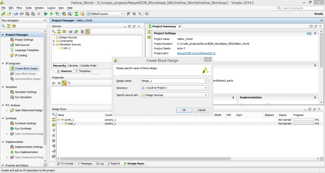
6. On the left you should see the Flow Navigator. Select Create Block Design under the IP Integrator. Give a name to your design without any empty spaces.
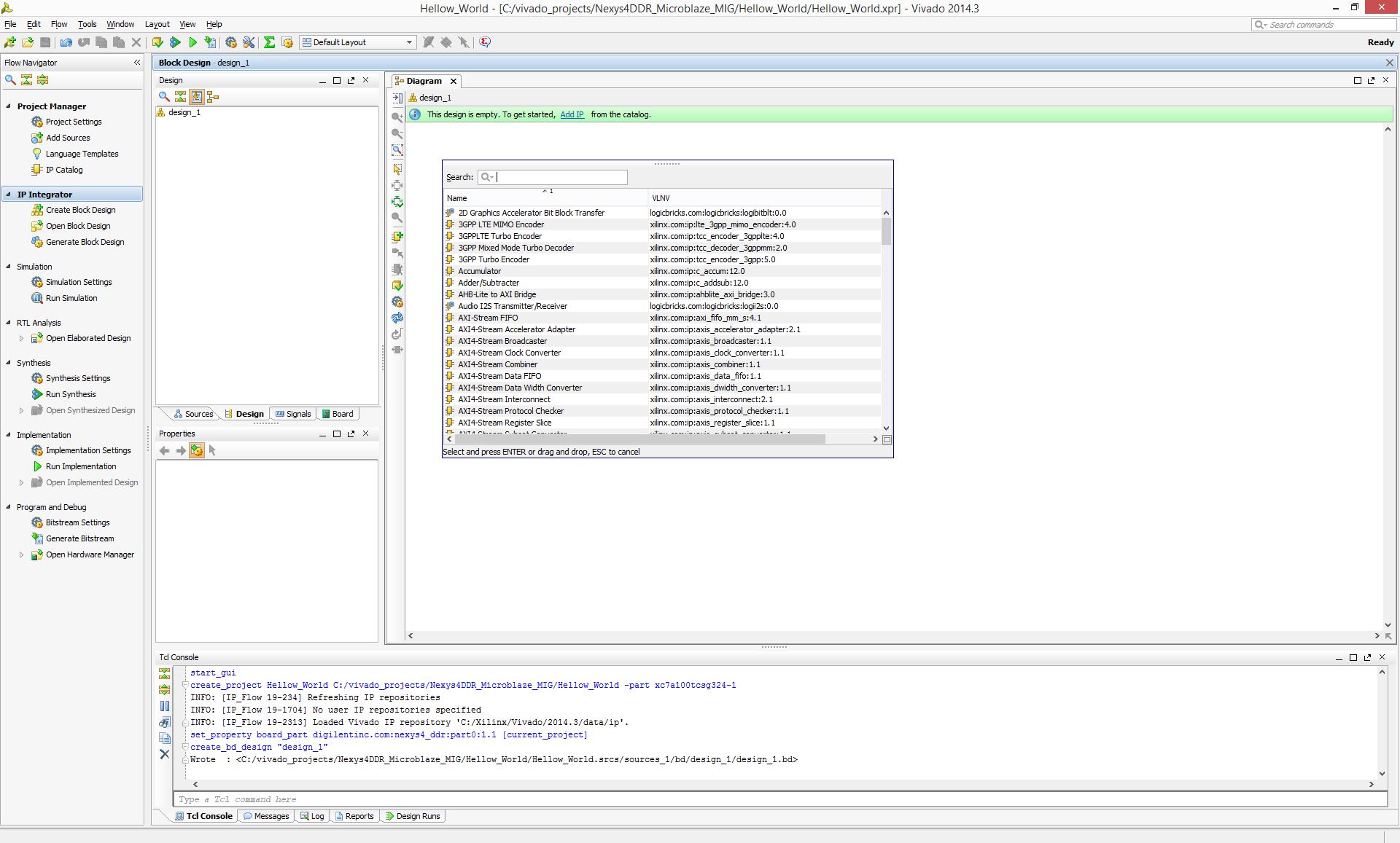
7. An empty design workspace is created where you can add IP blocks. You can click on the “Add IP” message prompt on the top or click on the yellow rectangular box with a green “+” on it. This should open a catalog of pre-built IP blocks from Xilinx IP repository. Search for “Microblaze” and double click on it to add the IP block to your empty design.
Adding Microblaze IP and Customization
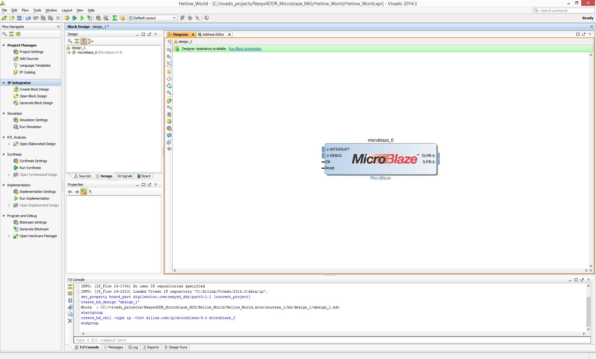
8. This is the Xilinx Microblaze IP block. When a new IP block is added the user can customize the block properties by either clicking on the “Run Block Automation” message prompt or by double clicking on the block itself.
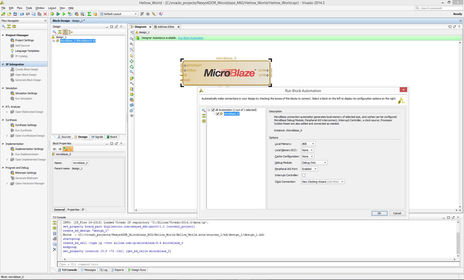
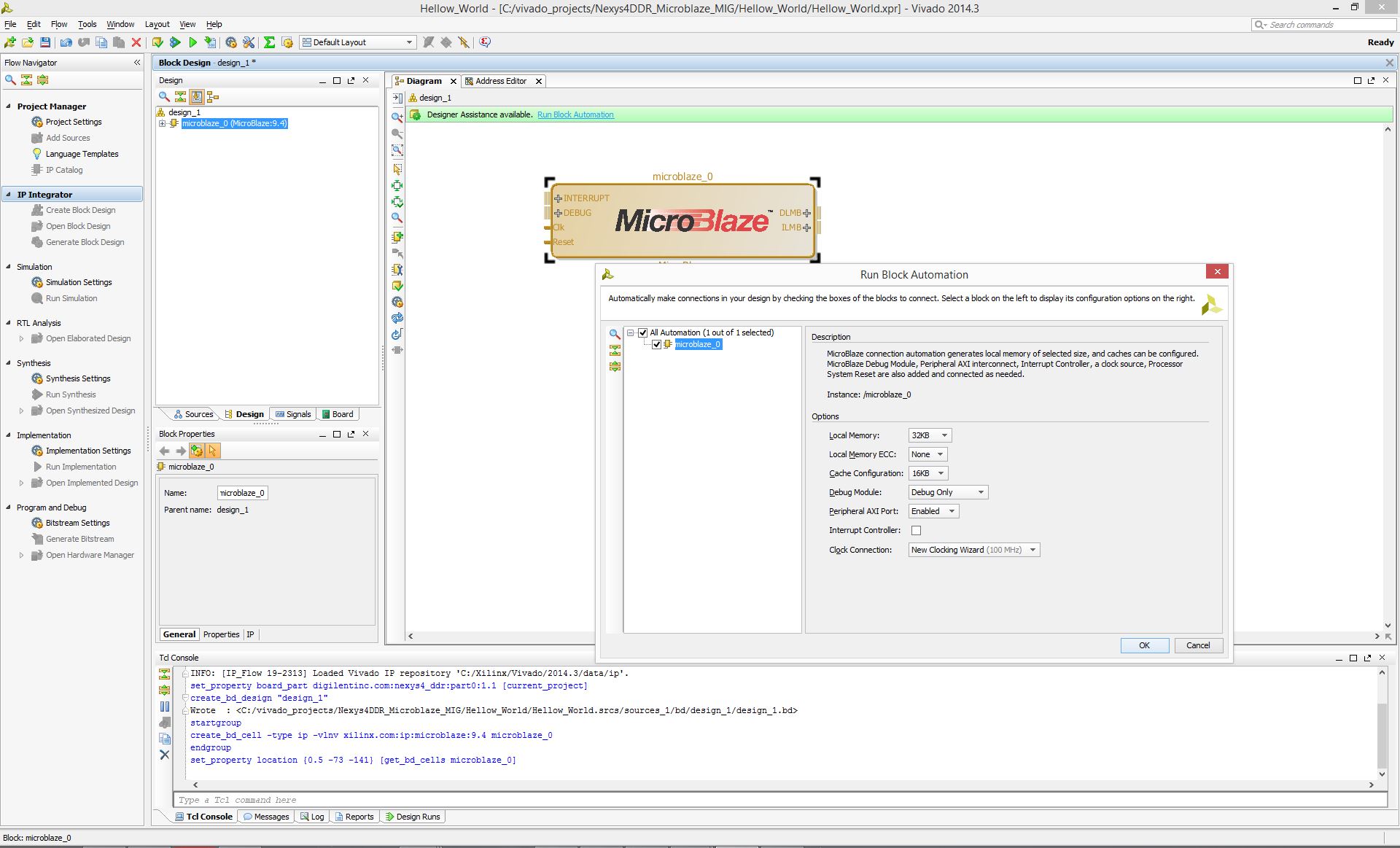
9. Run Block Automation and a customization assistant window will open with default settings.
10. Change default settings in the block options as shown below and click OK. This will customize the block with our new user settings.
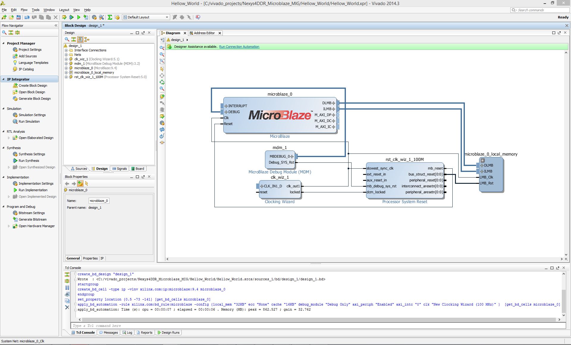
11. Running the block automation will auto-generate a set of additional IP blocks which will be added to our hardware design automatically based on the options selected in the previous step. Do not click on Run Connection Automation yet.
Customization of Clock Wizard IP Block
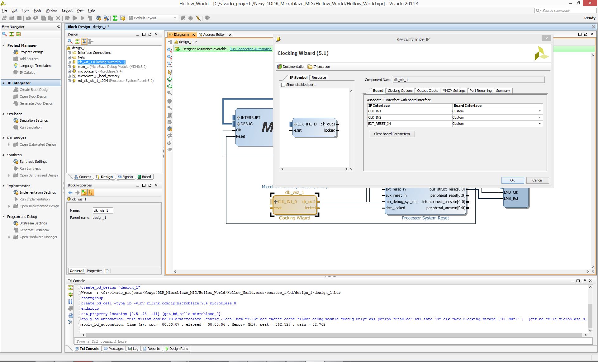
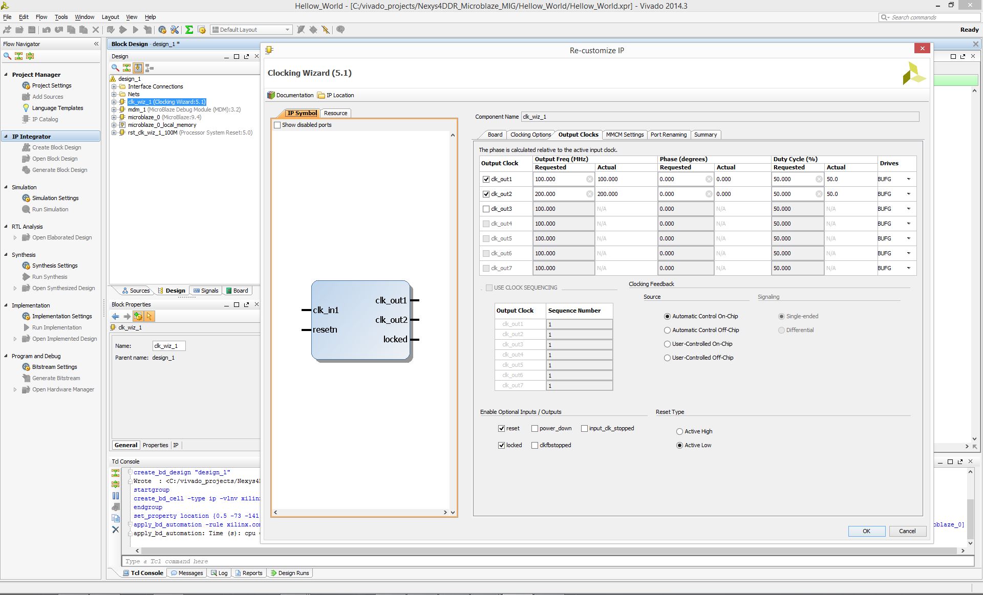
12. Double click on the Clock Wizard (clk_wiz_1) IP block.
13. Choose sys clock for CLK_IN1.
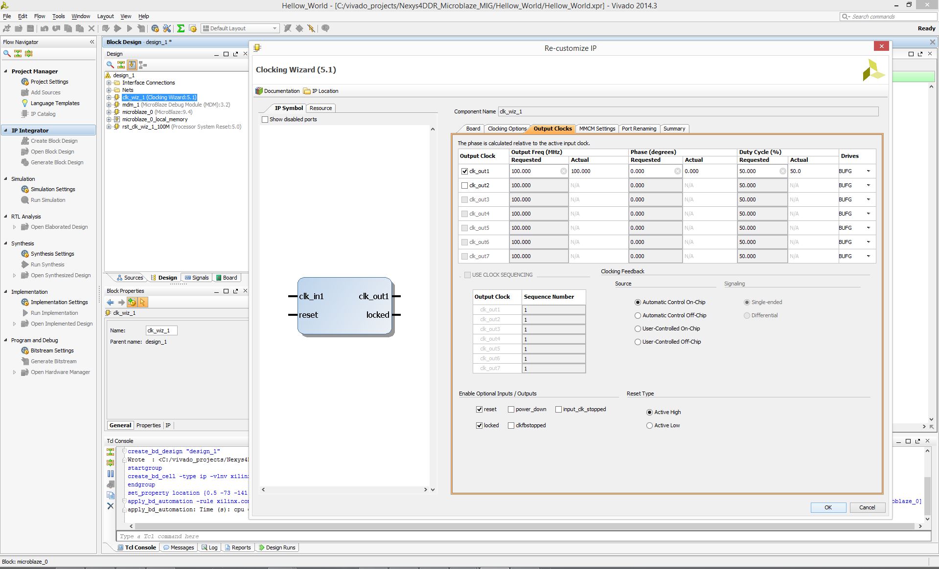
14. Select the Output Clocks tab.
15. Select clk_out2 output frequency as 200.000 (Mhz) and set Reset Type as Active Low. The left panel shows a GUI representation of the block and its internal settings. Observe that the reset pin will now read as resetn. This graphically represents the internal setting for active low.
16. Now move to the Port Renaming tab. This will give you a summary of the inputs and outputs to the Clock Wizard IP block.Click OK to finish block automation of Clock Wizard. Do not select Run Connection Automation yet.


