Cmod MX1 Reference Manual
The Cmod MX1 is retired and no longer for sale in our store.
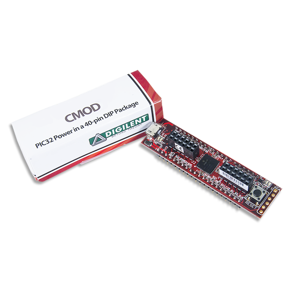
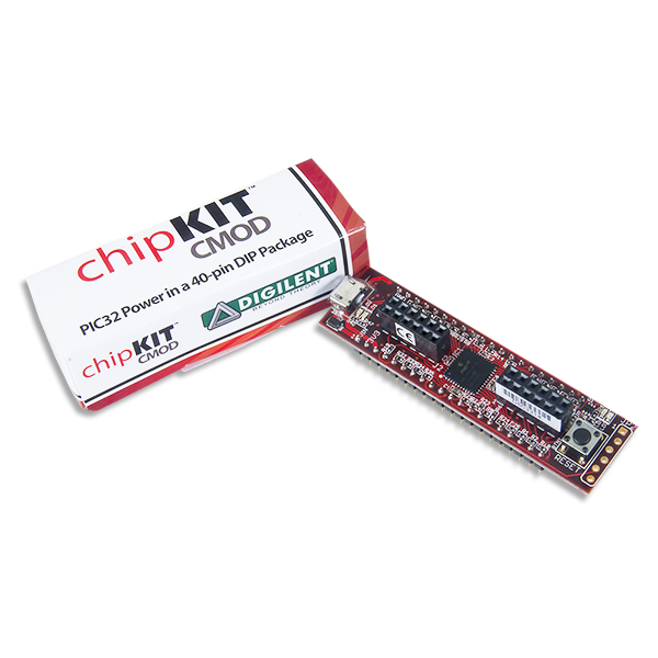
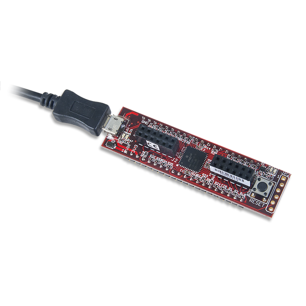
The Cmod MX1 is a MPIDE compatible board from Digilent. It combines a Microchip® PIC32MX150F128D microcontroller with a convenient 600-mil, 40-pin DIP package and two Digilent Pmod ports. Digilent’s Cmod boards are ideally suited for breadboards or other prototype circuit designs where the use of small surface mount packages is impractical.
The Cmod MX1 takes advantage of the powerful PIC32MX150F128D microcontroller. This microcontroller features a 32-bit MIPS processor core running at 40Mhz, 128K of flash memory, and 32K of SRAM data memory.
Download this reference manual
Features
- Microchip® PIC32MX150F128D microcontroller (40/50 Mhz 32-bit MIPS, 128K Flash, 32K SRAM)
- Convenient 600-mil, 2×20-pin DIP package
- 5V – 12V recommended operating voltage
- 33 available I/O pins
- Two user LEDs
- PC connection uses a USB A to micro B cable (not included)
- 13 analog inputs
- 3.3V operating voltage
- Two Pmod ports for Digilent peripheral module boards
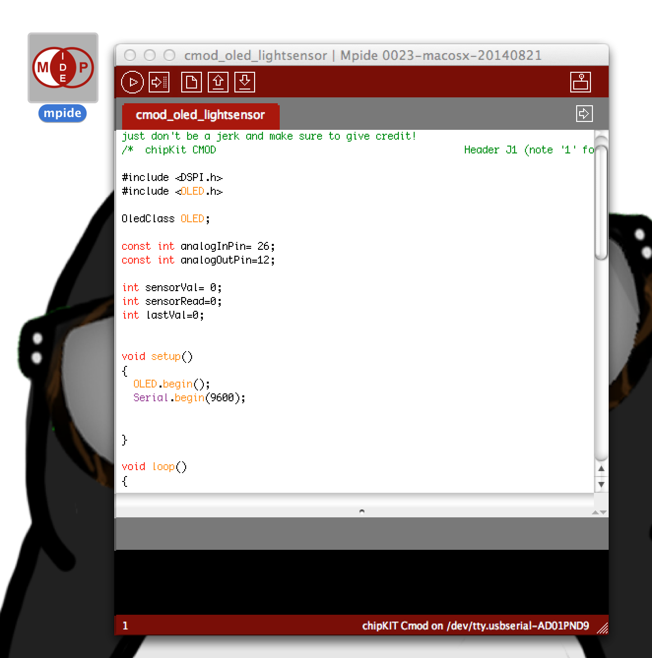
The Cmod MX1 can be programmed using the Multi-Platform Integrated Development Environment, MPIDE, an environment based on the open source Arduino IDE modified to support the PIC32 microcontroller. The board provides everything needed to start developing embedded applications using the MPIDE.
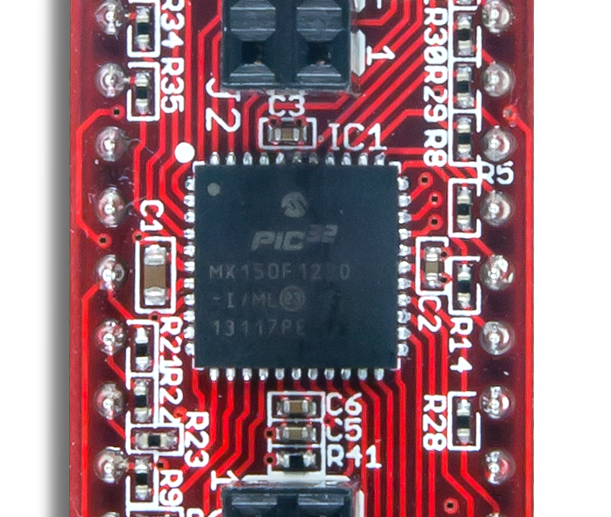
The Cmod MX1 is also fully compatible with the advanced Microchip MPLAB® IDE. To develop embedded applications using MPLAB®, a separate device programmer/debugger, such as the Digilent chipKIT PGM or the Microchip PICkit™3 is required.
1. Functional Description
The PIC32MX150F128D microcontroller features a 32-bit MIPS processor core capable of running at up to 50 MHz. When used with MPIDE, the Cmod MX1 operates the microcontroller at 40Mhz by default. The microcontroller features 128 KB of flash program memory and 32 KB of SRAM data memory. Programming the Cmod MX1 can be done using the Multi-Platform Integrated Development Environment (MPIDE) or with the advanced Microchip MPLAB® IDE with the addition of a PICKit3 or chipKIT PGM in-system programmer/debugger.
The Cmod MX1 provides 33 I/O pins located on the 40-pin DIP package. Some pins share functions with the onboard circuits such as the on-board LEDs, the UART data lines used by the USB serial converter, or the Pmod ports (see the schematic for details). If these peripherals are needed in the design, then the microcontroller can be reconfigured to allow these pins to be used for other purposes. Thirteen of the digital I/O pins can also be used as analog input pins.
The PIC32MX150F128D microcontroller supports peripheral functions such as UART, SPI, and I2C, as well as pulse-width-modulated outputs. To use the peripheral functions the PIC32MX1xx family of microcontrollers features a mappable I/O system called peripheral pin select (PPS), which allows select peripheral functionality to be mapped to multiple pins on the device. The default Cmod MX1 board support files provide a specific mapping of peripheral functions to microcontroller pins. This default pin mapping can be over-ridden by the user’s MPLABX program if a different mapping is desired (this requires the mentioned, compatible debugger).
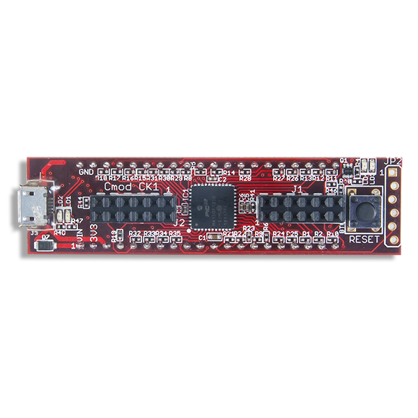
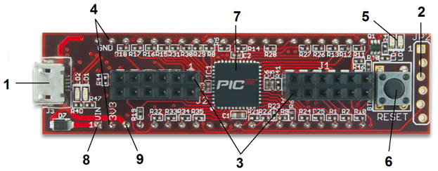
1.1. Hardware Overview
| Call Out | Component Description |
|---|---|
| 1 | J3 USB connector for USB serial converter |
| 2 | JP2 Microchip ICSP Connector |
| 3 | J1-J2 Digilent Pmod ports |
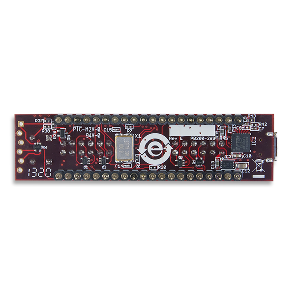
| 4 | 40 Pin DIP connector |
| 5 | User LEDs |
| 6 | Reset button |
| 7 | PIC32 Microcontroller |
| 8 | DIP Pin 1 external power connector |
| 9 | DIP Pin 3 USB 5.0V power connector |
2. Programming Tools
The Cmod MX1 can be used with either MPIDE or the Microchip MPLAB® development environment. When used with the MPLAB IDE, in-system programming and debugging of firmware running on the PIC32MX150 microcontroller is supported using an external programming/debugging circuit licensed from Microchip, such as the chipKIT PGM or the PICkit 2/3.
The Cmod MX1 is immediately usable with either the MPLAB IDE or the MPIDE.
2.1. MPIDE and USB Serial Communications
The Cmod MX1 board is designed to be used with the Multi-Platform IDE (MPIDE). The MPIDE development platform was created by modifying the Arduino™ IDE. It is backwards-compatible with the Arduino IDE.
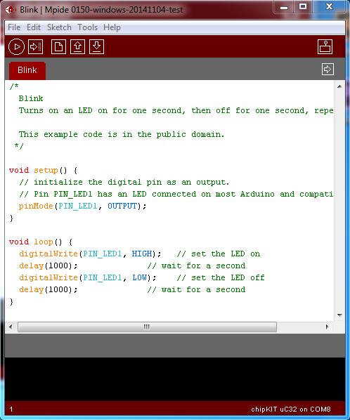
The MPIDE uses a serial communications port to communicate with a boot loader running on the Cmod MX1 board. The serial port on the board is implemented using an FTDI FT232R USB serial converter. Before attempting to use the MPIDE to communicate with the board, the appropriate USB device driver must be installed.
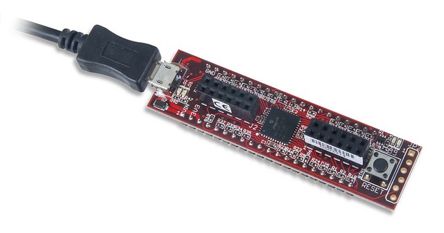
The Cmod MX1 uses a standard micro-USB connector for connection to a USB port on the PC. A USB-A to Micro-B cable, not supplied, is used to connect the board to a USB port on the host computer.
When the MPIDE needs to communicate with the Cmod MX1 board, the board is reset and starts running the boot loader. The MPIDE then establishes communications with the boot loader and downloads the program to the board.
When the MPIDE opens the serial communications connection on the PC, the DTR pin on the FT232R chip is driven low. This pin is coupled through a capacitor to the MCLR pin on the PIC32 microcontroller. Driving the MCLR line low resets the microcontroller, restarting execution with the boot loader. See the net labeled P32_RST in the schematic for further detail about this connection. The P32_RST net is also brought out to DIP pin 9.
Two red LEDs (LD1 and LD2) will blink when data is being sent or received between the Cmod MX1 and the PC over the serial connection.
2.2. Microchip Development Tool Compatibility
In addition to being used with the MPIDE, the Cmod MX1 board can be used as a more traditional microcontroller development board using Microchip's MPLAB development tool.

 Unloaded connector JP2 on the right side of the Reset button is used to connect to a Microchip development tool, such as the chipKIT PGM or the PICkit™3. The holes for JP2 are staggered so that a standard 100-mil spaced 6-pin header can press fit to the board without the need to solder it in place. Any Microchip development tool that supports the PIC32 microcontroller family can be used.
Typically, a right-angle male connector is used in JP2 so that the programmer can be attached coplanar with the Cmod MX1. The connector can be loaded from the top or the bottom. In either case, the programmer will be upside-down while the Cmod MX1 board is upright (button, LEDs, and Pmod ports visible). Ensure that pin 1 on the programmer is connected to the square solder pad on JP2. In some cases, because of mechanical clearance limitations, it may be necessary to use a 6-wire cable to connect a programmer to the chpKIT Cmod board.
The Microchip MPLAB® IDE or the MPLAB® X IDE can be used to program and debug code running on the Cmod MX1 board. These programs can be downloaded from the Microchip web site.
2.3. Reloading the Boot Loader
Using the Microchip development tools to program the board will cause the boot loader to be erased. To use the board with the MPIDE again, it is necessary to program the boot loader back onto the board. The boot loader compiled image can be found on the Cmod MX1 product page on the Digilent web site. The source code project for the boot loader is available on the Git server www.github.com.
To reprogram the boot loader using MPLAB X, perform the following steps:
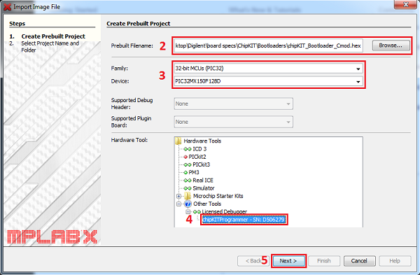
- Open MPLAB X, click on “File”, highlight “Import”, then select “HEX/ELF…(Prebuilt) File”

- Under “Prebuilt Filename”, click on the “Browse” button to locate the boot loader file that you downloaded previously. The file name should be something like “chipKIT_Bootloader_Cmod.hex”.
- Select “32-bit MCUs (PIC32)” in the “Family:” dialog box, then select the device ID “PIC32MX150F128D” in the “Device:” dialog box.
- With your board connected to the programmer and the programmer connected via USB cable to your PC, the programmer SN will load automatically under “Licensed Debugger” in the dialog box.
- Click the “Next” button at the bottom.
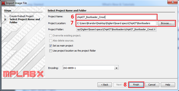
- Rename the project if you wish. The name of the .hex file is used by default.
- Choose where to place your project. The file where your boot loader is located is used by default.
- Click “Finish” to finalize the project file. The project will pop up in “Projects” tab on the left side of the screen.
- Right-click the project name and select “Make and Program Device”. The boot loader will now load to the Cmod. (You may also click the button on the tool bar with the green arrow pointing down to load the project if the project has been set as the main project.)

3. Power Supply
The Cmod MX1 is designed to be powered via USB (J3) or from an external power supply connected to pin 1 of the DIP package.
The Cmod MX1 has a single voltage regulator which regulates either 5V from USB, or a maximum of 15V external voltage. A series diode between the DIP pin 1 (VIN) and DIP pin 3 (USB5V0) prevents an external voltage applied to pin 1 being fed back onto the USB 5V supply when powering the board via DIP pin 1. All power supply options are regulated to 3.3 V to provide power to the VCC3V3 bus that powers the PIC32 microcontroller. The output of the on-board 3.3V regulator is available at DIP pin 2 and can be used to power external circuitry.
The 3.3V regulator is a Microchip MCP1703. The regulator is rated for a maximum output current of 250mA. The absolute maximum input voltage for the MCP1703 is 16V. This regulator has internal short circuit protection and thermal protection. It will get noticeably warm when the current consumed by the VCC3V3 bus is close to the 250mA maximum.
4. 5V Compatibility
The PIC32 microcontroller operates at 3.3V. There are two issues to consider when dealing with 5V compatibility for 3.3V logic. The first is protection of 3.3V inputs from damage caused by 5V signals. The second is whether the 3.3V output is high enough to be recognized as a logic high value by a 5V input. When driving a high impedance input (typical of CMOS logic), the output high voltage from the PIC32 microcontroller will be close to 3.3V. Some 5V devices will recognize this voltage as a logic high input, and some won’t. Many 5V logic devices will work reliably with 3.3V inputs. Please check the datasheet for the 5V components you are using to ensure that 3.3V will satisfy the logic high conditions for the components.
Some of the digital I/O pins on the PIC32 microcontroller are 5V tolerant. The analog capable I/O pins are not 5V tolerant. The following pins are 5V tolerant: 4-11, 14-15, 27, 31, and 33-38. The other pins are not 5V tolerant and 5V signals should not be applied to those pins. All I/O pins have a 200 ohm resistor in series between the microcontroller pin and the connector pins to provide short circuit protection. These resistors will limit the output drive strength of the pins to approximately +/- 2mA.
5. Pmod Ports
The Cmod MX1 has two ports for connecting Digilent Pmods. The Pmod ports, labeled J1 and J2, are 2×6, female pin header connectors.
The Pmod ports on the Cmod MX1 are both twelve-pin connectors. The ports use standard pin headers with 100-mil spaced pins. The twelve-pin ports have the pins in a 2×6 configuration.
The twelve-pin ports provide eight I/O signals, two 3.3V power pins, and two ground pins. The twelve-pin ports have the signals arranged so that one twelve-pin port is equivalent to two of the six-pin ports. Pins 1–4 and 7–10 are the signal pins, pins 5 and 11 are the ground pins, and pins 6 and 12 are the power supply pins.
The pin numbering that Digilent uses on the twelve-pin Pmod ports is non-standard.
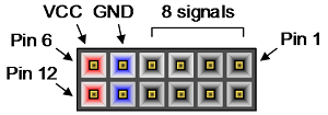
The upper row of pins are numbered 1–6, right to left (when viewed from the end of the connector), and the lower row of pins are numbered 7–12, right to left. This is in keeping with the convention that the upper and lower rows of pins can be considered to be two six-pin connectors stacked.
It is important to note that the Pmod ports on the Cmod MX1 are rotated 180 degrees in relation to each other. Pin 1 of each Pmod port is marked on the board. When viewing the top of the board, pin 1 of Pmod port J2 is the upper right pin, and pin 7 is immediately below it. For Pmod port J1, pin 1 is in the lower left corner and pin 7 is immediately above it. Connecting peripheral modules incorrectly could result in damaging the peripheral module or the Cmod MX1.

See the attached pinout diagram and tables in the appendices for more information about connecting peripheral modules and other devices to the Cmod MX1. These tables describe the mapping between pins on the PIC32MX150F128D microcontroller and the pins on the connectors.
6. Input/Output Connections
The Cmod MX1 board provides 33 of the I/O pins from the PIC32MX150F128D microcontroller to pins on the DIP connector.
The Cmod MX1 and the MPIDE system uses logical pin numbers to identify digital I/O pins. All digital I/O pins share their numbering with their DIP connector pin. Valid pin numbers on the Cmod MX1 are 4-8, 10-27, and 29-38. Pin numbers 1-3 and 39-40 refer to pins connected to power buses on the board and are not available for use as I/O. Pin 9 can be used to reset the PIC32 microcontroller and pin 28 is unconnected. In addition, several of these I/O pins share functionality with other devices on the board. See the attached pinout tables for more information.
The DIP connector uses standard DIP package pin numbers. Pins 1- 20 count up from the square pad labeled ‘1’ on the lower DIP connector. Pins 21-40 count up from the pin near the label ‘Q1’ to the pin labeled ‘GND’ on the other DIP connector.
Pins 18 and 19 are normally the reference voltages for the microcontroller’s A/D converter, but can also be used as digital I/O pins.
In addition to the connector pin, Pin 14 is also connected to the user LED LD3. Pin 12 also connects to the user LED LD4. (Note: When using MPIDE, LD3 is assigned to macro PIN_LED1 and LD4 is assigned to macro PIN_LED2.)
In addition to digital I/O, there are analog inputs available on the board, called A0 through A12. These pins are shared with digital pins 12, 13, and 16 through 26. Refer to the attached pinout tables for the correct mapping of these signals.
7. Peripheral I/O Functions
The PIC32 microcontroller on the board provides a number of peripheral functions. The following peripherals are provided:
I2C: Synchronous serial interface. The I2C1 interface is available on pins 4 (SDA1) and 38 (SCL1). The I2C2 interface is available on pins 22(SDA2) and 23(SCL2). Note that when using MPIDE, the only available I2C interface available is I2C1.
Note: The I2C bus uses open collector drivers to allow multiple devices to drive the bus signals. This means that pull-up resistors must be provided to supply the logic high state for the signals. These pull-up resistors are not on the Cmod MX1 board and must be provided externally. The required resistance of the pull-up resistor to use depends on the total number of devices on the bus, the length of wire, and the clock speed being used. It essentially depends on distributed capacitance on the bus. The higher the distributed capacitance and the faster the clock speed, the smaller the resistance should be. Values typically used are in the range of 2K to 10K ohms.
User LEDs: Pins 12 (LD4) and 14 (LD3). Both Pin 12 and Pin 14 are shared between a connector pin on the Cmod MX1 and an LED. Driving the pin high turns the LED on, driving it low turns it off. (Note: When using MPIDE, LD3 is assigned to macro PIN_LED1 and LD4 is assigned to macro PIN_LED2.)
External Interrupts: Only INT0 is hard-mapped on the microcontroller. It is connected to Pin 37 of the Cmod MX1. The other external interrupts are accessible via PPS described below.
A/D Converter Reference: Pin 18 is used to provide an external voltage reference to determine the input voltage range of the analog pins. The maximum voltage that can be applied to this pin is 3.3V. This pin can also be used as digital pin 18.
Reset: The PIC32 microcontroller is reset by bringing its MCLR pin low. The MCLR pin is connected to the P32_RST net on the circuit board. A reset button is located on the right side of the board. Pressing this button resets the PIC32 microcontroller.
Reset of the PIC32 microcontroller can be initiated by the USB serial converter. The USB serial converter brings the DTR pin low to reset the microcontroller. The P32_RST net is connected to Pin 9 of the DIP package. This allows external circuitry to reset the microcontroller, or to ensure that the circuitry is reset at the same time as the microcontroller.
8. Peripheral Pin Select
An advanced feature of the PIC32MX1xx/2xx families of microcontrollers is the ability to re-map the locations of peripheral devices. This advanced feature is available only in MPLAB® IDE or MPLAB® X. For more detailed information, refer to the PIC32MX1XX/2XX Data Sheet available from www.microchip.com.
The PPS Peripherals are pre-assigned to the following pins when programming the Cmod MX1 with MPIDE. These assignments are also included in the Notes sections of the attached pinout tables.
Output Compare: Pin 29 (OC1), Pin 38 (OC2), Pin 4 (OC3), Pin 22 (OC4), Pin 13 (OC5). Output compare allows for the implementation of pulse width modulated (PWM) signals using the analogWrite() function.
Input Capture: Pin 36 (IC1), Pin 10 (IC2), Pin 31 (IC3), Pin 37 (IC4), Pin 25 (IC5). Input capture allows for the synchronization of timers with captured signals, along with the execution of interrupts.
External Timer Input: Pin 30 (TCK1), Pin 18 (TCK2), Pin 27 (TCK3), Pin 32 (TCK4), Pin 26 (TCK5) allows for timers to be clocked from external sources.
External Interrupt: Pin 33 (INT1), Pin 13 (INT2), Pin 7 (INT3), Pin 37 (INT4) allows for external interrupts to be triggered in their own ISRs. Interrupts may be edge triggered or level triggered, though only one of rising, falling, high, or low, may be chosen for trigger sensitivity.
Change Notice Pins: All change notice pins are matched with their pin numbers (e.g. CN4 is associated with Pin 4). There is a change notice pin for each I/O pin.
UART: Asynchronous serial port. Pin 23 (U1TX), Pin 5 (U1RX). These pins use UART1 on the PIC32 microcontroller and are connected to the FT232RQ serial converter. It is possible to use these pins to connect to an external serial device when not using the USB serial interface. Pin 20 (U2TX) and Pin 21 (U2RX) are used to implement UART2 on the PIC32 microcontroller.
SPI: Synchronous serial port. Pin 24 (SS), Pin 35 (MISO), Pin 25 (MOSI), Pin 16 (SCK). This uses SPI1 on the PIC32 Microcontroller. SPI2 is implemented as Pin 33 (SS), Pin 36 (MOSI), Pin 32 (MISO), and Pin 17 (SCK).
When using the Cmod MX1 with MPIDE, the SPI ports are accessed using either the standard SPI library or using the Digilent DSPI library. The standard SPI library supports access to a single SPI port, SPI1. This is accessed using the SPI object. The DSPI library supports access to both SPI ports. The DSPI0 object class is used to access the default SPI port, SPI1. The DSPI1 object class is used to access SPI2.
Appendices
The following tables give the relationship between the digital pin numbers, the connector pin numbers, and the microcontroller pin numbers.
In the following tables, columns labeled pin # refer to the digital pin number. This is the value that is passed to the pinMode(), digitalRead(), digitalWrite(), and other functions to refer to the pin.
The signals mapped by using Peripheral Pin Select are included in the following tables. They are listed with the default pins assigned to them when using MPIDE. If the locations of peripheral devices are re-mapped, these signals may no longer be associated with the same pin as listed below.
Appendix A: Pinout Diagram
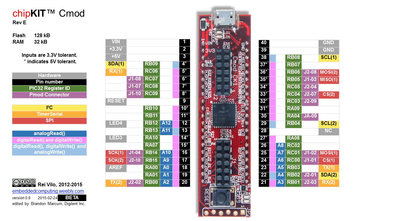
Appendix B: Pinout Table by DIP Connector/Pin Number
| DIP Pin # | Pin # | Connector Pin # | PIC32 Pin # | PIC32 Signal | Notes |
|---|---|---|---|---|---|
| 1 | - | - | - | N/A | VIN/External power |
| 2 | - | - | 28/40 | VDD | VCC3V3 |
| 3 | - | - | - | N/A | USB5V0/External 5V power for USB |
| 4 | 4 | - | 1* | RPB9/SDA1/CTED4/PMD3/RB9 | OC3 |
| 5 | 5 | - | 2* | RPC6/PMA1/RC6 | U1RX |
| 6 | 6 | J1-08 | 3* | RPC7/PMA0/RC7 | |
| 7 | 7 | J1-07 | 4* | RPC8/PMA5/RC8 | INT3 |
| 8 | 8 | J1-10 | 5* | RPC9/CTED7/PMA6/RC9 | |
| 9 | - | - | 18* | MCLR | Reset |
| 10 | 10 | - | 8* | PGED2/RPB10/CTED11/PMD2/RB10 | IC2 |
| 11 | 11 | - | 9* | PGEC2/RPB11/PMD1/RB11 | |
| 12 | 12/A12 | - | 10 | AN12/PMD0/RB12 | LD4 |
| 13 | 13/A11 | - | 11 | AN11/RPB13/CTPLS/PMRD/RB13 | OC5/INT2 |
| 14 | 14 | - | 12* | PGED(4)/TMS/PMA10/RA10 | LD3 |
| 15 | 15 | - | 13* | PGEC(4)/TCK/CTED8/PMA7/RA7 | |
| 16 | 16/A10 | J1-04 | 14 | CVREF/AN10/C3INB/RPB14/SCK1/CTED5/PMWR/RB14 | |
| 17 | 17/A9 | J2-10 | 15 | AN9/C3INA/RPB15/SCK2/CTED6/PMCS1/RB15 | |
| 18 | 18/A0 | - | 19 | VREF+/CVREF+/AN0/C3INC/RPA0/CTED1/RA0 | TCK2 |
| 19 | 19/A1 | - | 20 | VREF-/CVREF-/AN1/RPA1/CTED2/RA1 | |
| 20 | 20/A2 | J2-02 | 21 | PGED1/AN2/C1IND/C2INB/C3IND/RPB0/RB0 | U2TX |
| 21 | 21/A3 | J2-03 | 22 | PGEC1/AN3/C1INC/C2INA/RPB1/CTED12/RB1 | U2RX |
| 22 | 22/A4 | J2-01 | 23 | AN4/C1INB/C2IND/RPB2/SDA2/CTED13/RB2 | OC4 |
| 23 | 23/A5 | - | 24 | AN5/C1INA/C2INC/RTCC/RPB3/SCL2/RB3 | U1TX |
| 24 | 24/A6 | J1-01 | 25 | AN6/RPC0/RC0 | SS1 |
| 25 | 25/A7 | J1-02 | 26 | AN7/RPC1/RC1 | IC5/SDO1 |
| 26 | 26/A8 | - | 27 | AN8/RPC2/PMA2/RC2 | TCK5 |
| 27 | 27 | - | 32* | TDO/RPA8/PMA8/RA8 | TCK3 |
| 28 | - | - | - | - | Not connected |
| 29 | 29 | - | 33 | SOSCI/RPB4/RB4 | OC1 |
| 30 | 30 | J1-09 | 34 | SOSCO/RPA4/T1CK/CTED9/RA4 | TCK1 |
| 31 | 31 | - | 35* | TDI/RPA9/PMA9/RA9 | IC3 |
| 32 | 32 | J2-09 | 36 | RPC3/RC3 | TCK4/SDI2 |
| 33 | 33 | J2-07 | 37* | RPC4/PMA4/RC4 | INT1/SS2 |
| 34 | 34 | J2-04 | 38* | RPC5/PMA3/RC5 | |
| 35 | 35 | J1-03 | 41* | PGED3/RPB5/PMD7/RB5 | SDI1 |
| 36 | 36 | J2-08 | 42* | PGEC3/RPB6/PMD6/RB6 | IC1/SDO2 |
| 37 | 37 | - | 43* | RPB7/CTED3/PMD5/INT0/RB7 | IC4/INT4 |
| 38 | 38 | - | 44* | RPB8/SCL1/CTED10/PMD4/RB8 | OC2 |
| 39/40 | - | - | 6/16/29/39 | VSS/AVSS | GND |
* Indicates 5V tolerant pin on the PIC32MX150F128D
Appendix C: Pinout Table by Pmod Port Pin Number
| Connector Pin # | DIP Pin # | Pin # | PIC32 Pin # | PIC32 Signal | Notes |
|---|---|---|---|---|---|
| J1-01 | 24 | 24/A6 | 25 | AN6/RPC0/RC0 | SS1 |
| J1-02 | 25 | 25/A7 | 26 | AN7/RPC1/RC1 | IC5/SDO1 |
| J1-03 | 35 | 35 | 41* | PGED3/RPB5/PMD7/RB5 | SDI1 |
| J1-04 | 16 | 16/A10 | 14 | CVREF/AN10/C3INB/RPB14/SCK1/CTED5/PMWR/RB14 | |
| J1-05 | 39/40 | - | 6/16/29/39 | VSS/AVSS | GND |
| J1-06 | 2 | - | 28/40 | VDD | VCC3V3 |
| J1-07 | 7 | 7 | 4* | RPC8/PMA5/RC8 | INT3 |
| J1-08 | 6 | 6 | 3* | RPC7/PMA0/RC7 | |
| J1-09 | 30 | 30 | 34 | SOSCO/RPA4/T1CK/CTED9/RA4 | TCK1 |
| J1-10 | 8 | 8 | 5* | RPC9/CTED7/PMA6/RC9 | |
| J1-11 | 39/40 | - | 6/16/29/39 | VSS/AVSS | GND |
| J1-12 | 2 | - | 28/40 | VDD | VCC3V3 |
| J2-01 | 22 | 22/A4 | 23 | AN4/C1INB/C2IND/RPB2/SDA2/CTED13/RB2 | OC4 |
| J2-02 | 20 | 20/A2 | 21 | PGED1/AN2/C1IND/C2INB/RPB0/RB0 | U2TX |
| J2-03 | 21 | 21/A3 | 22 | PGEC1/AN3/C1INC/RPB1/CTED12/RB1 | U2RX |
| J2-04 | 34 | 34 | 38* | RPC5/PMA3/RC5 | |
| J2-05 | 39/40 | - | 6/16/29/39 | VSS/AVSS | GND |
| J2-06 | 2 | - | 28/40 | VDD | VCC3V3 |
| J2-07 | 33 | 33 | 37* | RPC4/PMA4/RC4 | INT1/SS2 |
| J2-08 | 36 | 36 | 42* | PGEC3/RPB6/PMD6/RB6 | IC1/SDO2 |
| J2-09 | 32 | 32 | 36 | RPC3/RC3 | TCK4/SDI2 |
| J2-10 | 17 | 17/A9 | 15 | AN9/C3INA/RPB15/SCK1/CTED6/PMCS1/RB15 | |
| J2-11 | 39/40 | - | 6/16/29/39 | VSS/AVSS | GND |
| J2-12 | 2 | - | 28/40 | VDD | VCC3V3 |
| - | 1 | - | - | N/A | VIN/External power |
| - | 3 | - | - | N/A | USB5V0/External 5V power for USB |
| - | 4 | 4 | 1* | RPB9/SDA1/CTED4/PMD3/RB9 | OC3 |
| - | 5 | 5 | 2* | RPC6/PMA1/RC6 | U1RX |
| - | 9 | 18* | MCLR | Reset Button | |
| - | 10 | 10 | 8* | PGED2/RPB10/CTED11/PMD2/RB10 | IC2 |
| - | 11 | 11 | 9* | PGEC2/RPB11/PMD1/RB11 | |
| - | 12 | 12/A12 | 10 | AN12/PMD0/RB12 | LD4 |
| - | 13 | 13/A11 | 11 | AN11/RPB13/CTPLS/PMRD/RB13 | OC5/INT2 |
| - | 14 | 14 | 12* | PGED(4)/TMS/PMA10/RA10 | LD3 |
| - | 15 | 15 | 13* | PGEC(4)/TCK/CTED8/PMA7/RA7 | |
| - | 18 | 18/A0 | 19 | VREF+/CVREF+/AN0/C3INC/RPA0/CTED1/RA0 | TCK2 |
| - | 19 | 19/A1 | 20 | VREF-/CVREF-/AN1/RPA1/CTED2/RA1 | |
| - | 23 | 23/A5 | 24 | AN5/C1INA/C2INC/RTCC/RPB3/SCL2/RB3 | U1TX |
| - | 26 | 26/A8 | 27 | AN8/RPC2/PMA2/RC2 | TCK5 |
| - | 27 | 27 | 32* | TDO/RPA8/PMA8/RA8 | TCK3 |
| - | 28 | - | - | - | Not connected |
| - | 29 | 29 | 33 | SOSCI/RPB4/RB4 | OC1 |
| - | 31 | 31 | 35* | TDI/RPA9/PMA9/RA9 | IC3 |
| - | 37 | 37 | 43* | RPB7/CTED3/PMD5/INT0/RB7 | IC4/INT4 |
| - | 38 | 38 | 44* | RPB8/SCL1/CTED10/PMD4/RB8 | OC2 |
* Indicates 5V tolerant pin on the PIC32MX150F128D
Appendix D: Pinout Table by PIC32 Microcontroller Pin
| PIC32 Pin # | DIP Pin # | Pin # | Connector Pin # | PIC32 Signal | Notes |
|---|---|---|---|---|---|
| 1* | 4 | 4 | - | RPB9/SDA1/CTED4/PMD3/RB9 | OC3 |
| 2* | 5 | 5 | - | RPC6/PMA1/RC6 | U1RX |
| 3* | 6 | 6 | J1-08 | RPC7/PMA0/RC7 | |
| 4* | 7 | 7 | J1-07 | RPC8/PMA5/RC8 | INT3 |
| 5* | 8 | 8 | J1-10 | RPC9/CTED7/PMA6/RC9 | |
| 6 | 39/40 | - | - | VSS/AVSS | GND |
| 7 | VCAP | ||||
| 8* | 10 | 10 | - | PGED2/RPB10/CTED11/PMD2/RB10 | IC2 |
| 9* | 11 | 11 | - | PGEC2/RPB11/PMD1/RB11 | |
| 10 | 12 | 12/A12 | - | AN12/PMD0/RB12 | LD4 |
| 11 | 13 | 13/A11 | - | AN11/RPB13/CTPLS/PMRD/RB13 | OC5/INT2 |
| 12* | 14 | 14 | - | PGED(4)/TMS/PMA10/RA10 | LD3 |
| 13* | 15 | 15 | - | PGEC(4)/TCK/CTED8/PMA7/RA7 | |
| 14 | 16 | 16/A10 | J1-04 | CVREF/AN10/C3INB/RPB14/SCK1/CTED5/PMWR/RB14 | |
| 15 | 17 | 17/A9 | J2-10 | AN9/C3INA/RPB15/SCK2/CTED6/PMCS1/RB15 | |
| 16 | 39/40 | - | - | VSS/AVSS | GND |
| 17 | AVDD | ||||
| 18* | 9 | - | - | MCLR | Reset |
| 19 | 18 | 18/A0 | - | VREF+/CVREF+/AN0/C3INC/RPA0/CTED1/RA0 | TCK2 |
| 20 | 19 | 19/A1 | - | VREF-/CVREF-/AN1/RPA1/CTED2/RA1 | |
| 21 | 20 | 20/A2 | J2-02 | PGED1/AN2/C1IND/C2INB/C2IND/RPB0/RB0 | U2TX |
| 22 | 21 | 21/A3 | J2-03 | PGEC1/AN3/C1INC/C2INA/RPB1/CTED12/RB1 | U2RX |
| 23 | 22 | 22/A4 | J2-01 | AN4/C1INB/C2IND/RPB2/SDA2/CTED13/RB2 | OC4 |
| 24 | 23 | 23/A5 | - | AN5/C1INA/C2INC/RTCC/RPB3/SCL2/RB3 | U1TX |
| 25 | 24 | 24/A6 | J1-01 | AN6/RPC0/RC0 | SS1 |
| 26 | 25 | 25/A7 | J1-02 | AN7/RPC1/RC1 | IC5/SDO1 |
| 27 | 26 | 26/A8 | - | AN8/RPC2/PMA2/RC2 | TCK5 |
| 28 | 2 | - | - | VDD | VCC3V3 |
| 29 | 39/40 | - | - | VSS/AVSS | GND |
| 30 | OSC1/CLKI/RPA2/RA2 | X1, system clock oscillator | |||
| 31 | OSC2/CLKO/RPA3/RA3 | X1, system clock oscillator | |||
| 32* | 27 | 27 | - | TDO/RPA8/PMA8/RA8 | TCK3 |
| 33 | 29 | 29 | - | SOSCI/RPB4/RB4 | OC1 |
| 34 | 30 | 30 | J1-09 | SOSCO/RPA4/T1CK/CTED9/RA4 | TCK1 |
| 35* | 31 | 31 | - | TDI/RPA9/PMA9/RA9 | IC3 |
| 36 | 32 | 32 | J2-09 | RPC3/RC3 | TCK4/SDI2 |
| 37* | 33 | 33 | J2-07 | RPC4/PMA4/RC4 | INT1/SS2 |
| 38* | 34 | 34 | J2-04 | RPC5/PMA3/RC5 | |
| 39 | 39/40 | - | - | VSS/AVSS | GND |
| 40 | 2 | - | - | VDD | VCC3V3 |
| 41* | 35 | 35 | J1-03 | PGED3/RPB5/PMD7/RB5 | SDI1 |
| 42* | 36 | 36 | J2-08 | PGEC3/RPB6/PMD6/RB6 | IC1/SDO2 |
| 43* | 37 | 37 | - | RPB7/CTED3/PMD5/INT0/RB7 | IC4/INT4 |
| 44* | 38 | 38 | - | RPB8/SCL1/CTED10/PMD4/RB8 | OC2 |
| - | 1 | - | - | N/A | VIN/external power |
| - | 3 | - | - | N/A | USB5V0/external 5V power for USB |
| - | 28 | - | - | N/A | Not connected |
* Indicates 5V tolerant pin on the PIC32MX150F128D

