Basys MX3 Reference Manual
The Basys MX3 is retired and no longer for sale in our store.
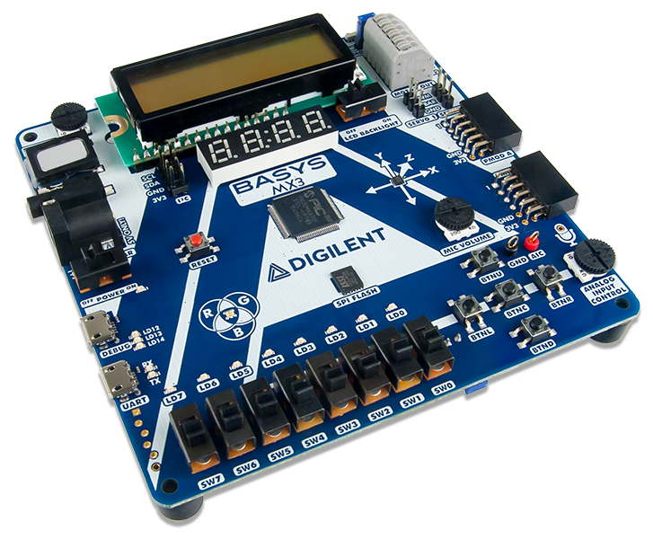
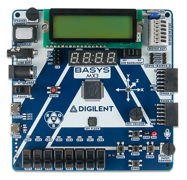
The Basys MX3 is a true MCU trainer board designed from the ground up around the teaching experience. Basys MX3 features the PIC32MX370 from Microchip and was designed to be used with the MPLAB® X IDE. With an exhaustive set of peripherals, students gain exposure to a wide range of embedded systems related concepts while using a professional grade tool set. Accompanied by free and open source coursework, including seven in-depth teaching units and 15 complete labs, the Basys MX3 is a versatile MCU trainer board ideal for teaching introductory embedded systems courses.

Download This Reference Manual
Features
- PIC32MX370F512L Microcontroller
- MIPS32® M4K® core runs up to 96 MHz using onboard 8 MHz oscillator
- 512 KB of Program Flash Memory, 12 KB of Boot Flash Memory
- 128 KB of SRAM
- Four Direct Memory Access (DMA) Modules
- Two SPI, Two I²C, and Five UART serial interfaces
- Parallel Master Port (PMP) for graphics interfaces
- Five 16-bit Timers/Counters
- Five Input Capture Modules
- Five Output Compare Modules
- 85 I/O pins
- 54 pins support Peripheral Pin Select (PPS) for function remapping
- Power
- Powered from USB or any 5V external power source
- USB and Debugging
- USB-UART Bridge
- USB programmer/debugger
- 30-pin Analog Discovery 2 connector
- Switches, Push-buttons, LEDs and Displays
- 5 Push-buttons
- 1 Reset button
- 8 Slide switches
- 8 LEDs
- 1 RGB LED
- 4 Digit 7-segment display
- LCD character display
- Audio, Motor control, and other devices
- Speaker with Audio Output Jack and volume control
- Microphone with volume control
- Dual H-Bridge Motor Driver for up to two 1.5 A Brushed DC Motors or one stepper motor
- 2 Servo Connectors
- FIR-compatible IrDA Module
- Potentiometer
- 3-axis, 12-bit accelerometer
- 4 MB SPI Flash
- Expansion Connectors
- Two standard Pmod ports
- 16 Total microcontroller I/O
- One I2C Connector
- 2 Total microcontroller I/O


Software Support
The Basys MX3 is fully supported by Microchip’s MPLAB X IDE. See section 1 on Programming the Board for more information on using the Basys MX3 in MPLAB X IDE. Digilent provides a set of libraries called the Basys MX3 Library Pack that adds support for all onboard peripherals. This library pack can be downloaded from the Basys MX3 Resource Center. The users may choose to implement their own functionality in order to access Basys MX3 resources.
The Basys MX3 can also be used in Arduino IDE once the Digilent Core for Arduino IDE has been installed. Instructions for installing the Digilent Core for Arduino IDE can be found on the Basys MX3 Resource Center.
Coursework and Additional Materials
Basys MX3 comes with a complete set of coursework designed to give teaching professionals flexibility in designing embedded systems and other microprocessor courses. With almost 300 pages of material, “Embedded Systems Basys MX3 and PIC32MX370” covers topics from toggling LEDs, motor control, and introduction to digital signal processing. Access to the full coursework is available on the Basys MX3 Resource Center.
Links to additional materials from Digilent and Microchip, including the Basys MX3 schematic and the PIC32MX370F512L datasheet, can also be found on the Basys MX3 Resource Center.
The Basys MX3 uses a lot of devices to implement all of the functionality it provides (accelerometer, flash memory, motor driver, IRDA, etc.). The manufacturers of each of these devices provide detailed descriptions of their functionality in their datasheets.
1. Programming the Board
1.1. Programming Tools
The Basys MX3 can be used with Microchip’s standard MPLAB X IDE. This software suite can be downloaded for free from the Microchip website and includes a free evaluation copy of the XC32 compiler for use with the PIC32 microcontroller family.
MPLAB X IDE is the tool used to write, compile, program, and debug code running on the Basys MX3 board. Programming and debugging a program on the Basys MX3 using the MPLAB X IDE is possible using the DEBUG USB connector. The board contains all the required circuitry for MPLAB X to communicate with the onboard PIC32, so no additional programming tools need to be purchased.
When creating a new project in MPLAB X, a wizard allows you to setup the environment and device specific tools. The steps for this include the following:
- Select Microchip Embedded / Standalone Project, then use the “Select Device” option to specify the PIC32 microcontroller being used: PIC32MX370F512L.
- Select the programming tool named Basys MX3 corresponding to the board you want to program, under Licensed Debugger group.

- Select the compiler you want to use.

Another useful tool included with MPLAB X is MPLAB X IPE. This tool allows the direct programming/erasing of the microcontroller, but it does not provide an environment for writing, compiling, and debugging the code. Please see Microchip documentation for instructions on using this tool.
1.2. Programming Basics
It is often very helpful to include the xc.h header when writing code for the Basys MX3:
#include <xc.h>
This further provides the inclusion of another header (p32mx370f512l.h) into the project that provides useful definitions such as:
- Register names
- example (register LATA is set to 0):
LATA = 0;
- Specific register bits that can be accessed using a structure having the name of the register suffixed by “bits”.
- example (bit LATA1 of the register LATA is set to 1):
LATAbits.LATA1 = 1;
Digilent provides a set of libraries called the Basys MX3 Library Pack that addresses much of the functionality on the Basys MX3:
- ACL (accelerometer)
- ADC (Analog to Digital converter)
- AUDIO
- BTN (buttons)
- IRDA
- LCD
- LED
- MIC (microphone)
- MOT (motors)
- PMODS
- RGBLED
- SPIFLASH
- SSD
- SWT (Switches)
- UART
These libraries are wrappers over the lower level functions that access the registers, allowing the user to call the functionality using functions like:
LED_Init();
LED_SetValue(4, 1); //turn on LED4
This set of libraries comes with the user documentation, but basically this is what you have to do in order to use them:
- Include in your project the .c and .h files corresponding to the module you want to use (for example led.c and led.h).
- In your code, include the header of the module:
#include "led.h"
- In your code, call the needed functions
1.3. Digital Inputs and Outputs
The PIC32MX370F512L microcontroller offers access to all the board resources through its pins, so understanding how to access their features is very important. The list that describes each pin functionality is included in Appendix 3. You can see that each pin may have multiple functions, but all pins have one feature in common: they have an associated digital I/O (input/output) bit. On PIC32 microcontrollers, the I/O pins are grouped into I/O Ports and are accessed via peripheral registers in the microcontroller. There are seven I/O Ports numbered A–G and each is 16 bits wide. Depending on the PIC32 microcontroller, some of the I/O Ports are not present, and not all 16 bits are accessible in all I/O Ports.
Each I/O Port has the following control registers: TRIS, LAT, PORT, ANSEL, CNPU, CNPD, and ODC. The registers for each I/O Port are named after it: TRISx, LATx, PORTx, ANSELx, CNPUx, CNPDx and ODCx. For example, port A will have the following assigned registers: TRISA, LATA, etc.
The TRIS register is used to set the pin direction. Setting a TRIS bit to 0 makes the corresponding pin an output. Setting the TRIS bit to 1 makes the pin an input.
The LAT register is used to write to the I/O Port. Writing to the LAT register sets any pins configured as outputs. Reading from the LAT register returns the last value written.
The PORT register is used to read from the I/O Port. Reading from the PORT register returns the current state of all the pins in the I/O Port. Writing to the PORT register may not produce the expected result, therefore writing to LAT register is recommended.
To summarize: write using LAT, read using PORT.
PIC32 microcontrollers allow any pin set as an output to be configured as either a normal digital output or as an open-drain output. The ODC register is used to control the output type. Setting an ODC bit to 0 makes the pin a normal output and setting it to 1 makes the pin an open-drain output.
The multifunction pins that include analog input functionality need to be configured in order to be used as digital pins by clearing the corresponding bit from ANSEL register. These pins will include ANx in their name. For example: AN11/PMA12/RB11 for RB11.
This microcontroller has a weak pull-up and a weak pull-down connected to each pin. These pull-ups and pull-downs are enabled/disabled by setting the corresponding bits from CNPU and CNPD registers to 1/0. The default setting is 0 (pull-ups and pull-downs disabled).
You can see a typical example of I/O pin configuration as output and digital output operations in the User LEDs section.
You can see a typical example of I/O pin configuration as input (including analog disable) and digital input operations in the User Buttons section.
Refer to the PIC32MX3XX/4XX Family Datasheet, and the PIC32 Family Reference Manual, Section 12, IO Ports, for more detailed information about the operation of the I/O Ports in the microcontroller.
1.4. Remappable pins
Users may independently map the input and/or output of most digital peripherals to a fixed subset of digital I/O pins. Pins that support the peripheral pin select feature include the designation “RPn” in their full pin designation, where “RP” designates a remappable peripheral and “n” is the remappable port number.
The available peripherals to be mapped are digital-only. These include general serial communications (UART and SPI), general purpose timer clock inputs, timer-related peripherals (input capture and output compare), and interrupt-on-change inputs.
On the other hand, some peripheral modules cannot be included in the peripheral pin select feature because it requires special I/O circuitry on a specific port and it cannot be easily connected to multiple pins. These modules include I2C and analog-to-digital converters (ADC), among others.
Peripheral pin select features are controlled using two sets of Special Function Registers (SFRs): one to map peripheral inputs, and one to map peripheral outputs.
The peripheral inputs are mapped and named from the peripheral perspective (based on the peripheral). The [pin name]R registers, where [pin name] refers to the specific peripheral pins, are used to configure peripheral input mapping. TABLE 12-1 in the PIC32MX370F512L datasheet from Microchip (and Appendix 1 in this document) shows the different pins and their values available to assign to a peripheral pin.
The following example shows how different I/Os, such as pin RF4, can be assigned to U1RX input pin of the UART1 peripheral:
U1RXR = 0x02; // 0010 corresponds to RF4

The peripheral outputs are mapped and named from the pin perspective (on the basis of the pin). The RPnR registers (Register 12-2) are used to control output mapping. The PIC32MX370F512L datasheet details in TABLE 12-2 (and Appendix 2 in this document) the values corresponding to each IO pin, associated to each available peripheral pin. Note that the current version of the Basys MX3 schematic (B.0) incorrectly lists RD6 and RD7 as remappable pins (RPD6 and RPD7, respectively); these pins are not remappable on the PIC32MX370F512L.
The following example shows how different peripheral outputs, such as U3TX, can be assigned to pin RF4:
RPF4R = 0x01; // 0001 corresponds to U3TX

Input and output remapping is illustrated in the SPI2 section, where the SPI2 pins are mapped over the pins of PMOD A connector.
1.5. CPU Clock Source
The PIC32 microcontroller supports numerous clock source options for the main processor operating clock. The Basys MX3 uses an 8MHz external crystal for use with the XT oscillator option. Oscillator options are selected via the configuration settings specified using the
#pragma config
statement. Use
#pragma config POSCMOD=XT
to select the XT option.
Using the internal system clock phase-locked loop (PLL), it is possible to select numerous multiples or divisions of the 8MHz oscillator to produce CPU operating frequencies up to 80MHz. The clock circuit PLL provides an input divider, multiplier, and output divider. The external clock frequency (8MHz) is first divided by the input divider value selected. This is multiplied by the selected multiplier value and then finally divided by the selected output divider. The result is the system clock, SYSCLK, frequency. The SYSCLK frequency is used by the CPU, DMA controller, interrupt controller, and pre-fetch cache.
The values controlling the operating frequency are specified using the PIC32MX370 configuration variables. These are set using the #pragma config statement. Use
#pragma config FPLLIDIV
to set the input divider,
#pragma config FPLLMUL
to set the multiplication factor and
#pragma config FPLLODIV
to set the output divider. Refer to the PIC32MX3XX/4XX Family Data Sheet and the PIC32MX Family Reference Manual, Section Oscillators, for information on how to choose the correct values, as not all combinations of multiplication and division factors will work.
In addition to configuring the SYSCLK frequency, the peripheral bus clock, PBCLK, frequency is also configurable. The peripheral bus clock is used for most peripheral devices, and in particular is the clock used by the timers, and serial controllers (UART, SPI, I2C). The PBLCK frequency is a division of the SYSCLK frequency selected using
#pragma config FPBDIV
The PBCLK divider can be set to divide by 1, 2, 4, or 8.
The following example will set up the Basys MX3 for operation with a SYSCLK frequency of 80MHz and a PBCLK frequency of 80MHz.
#pragma config FNOSC =	FRCPLL
#pragma config FSOSCEN =	OFF
#pragma config POSCMOD =	XT
#pragma config OSCIOFNC =	ON
#pragma config FPBDIV =     DIV_1

#pragma config FPLLIDIV =	DIV_2
#pragma config FPLLMUL =	MUL_20
#pragma config FPLLODIV =	DIV_1
2. Power Supplies
The Basys MX3 requires a 5-volt power source to operate. This power source can come from the Programming / Debugging USB port (J12), the USB-UART (J10), or from an external 5 Volt DC power supply that’s connected to Power Jack (J11). These three power inputs are connected together through Schottky diodes to form the primary input power network, VIN, which is used to power the onboard regulators and the majority of the onboard peripherals. No jumper is required to select the input power source. The board will automatically power on while the Power Switch (SW8) is in the on position and power is present on any of the power inputs.
A power-good LED (LD11), driven by the output of the 3.3 volt regulator (LMR10515), indicates that the board is receiving power and that the on-board supplies are functioning as expected. An overview of the Basys MX3 power circuit is shown in Fig. 2.1.

The USB port(s) can deliver enough power for the vast majority of designs. However, a few demanding applications, including any that drive multiple peripheral boards, may require more power than a USB port is capable of providing. In these instances an external power supply can be used. Due to their high current demands motors and servos cannot be powered through either of the USB ports, and may only be powered through an external supply.
An external power supply can be used by plugging into Power Jack J11. The supply must use a coaxial, center-positive 2.0 mm internal-diameter plug, and provide a voltage of 5 Volts DC (4.75 Volts minimum, 5.5 Volts maximum). The supply should provide a minimum current of 2 amps if servos are to be used. Ideally, the supply should be capable of provide 20 Watts of power (5 Volts DC, 4 amps). Many suitable supplies can be purchased from Digilent or other catalog vendors.
The on-board Motor Driver (Texas Instruments DRV8835) may be powered by a 5 Volt supply connected to Power Jack J11 or by an external supply (0 Volts to 11 Volts) connected to pins 1 and 2 of Terminal Block J5. Jumper JP1 is used to select which power source is used by the Motor Driver.
Table 2.1. Power rail characteristics.
| Supply | Circuit | Device | Current (max/typical) |
|---|---|---|---|
| 3.3V (VCC3V3) | PIC32MX370, Pmods, and all on-board peripherals excluding the LCD backlight, RGB LED, IrDA LED, Servos, and Motors | IC10: Texas Instruments LMR10515 | 1.5A/NA |
| 3.3V (DBG3V3) | Onboard Microchip Programmer/Debugger | IC11: Texas Instruments LP2985IM5-3.3 | 150mA/NA |
3. User LEDs
Eight LEDs are provided, labeled LD0 – LD7 on the board (and LED0 – LED7 on the schematic), attached to eight digital IO pins. Controlling the LEDs is done by basic access to an output IO pin. Read more details in the Digital Inputs and Outputs chapter.

Figure 3.1 shows the way the LEDs are electrically connected on the Basys MX3.
3.1. Connectivity
Table 3.1. LED connectivity.
| Label | Schematic Name | PIC32 Pin | Description |
|---|---|---|---|
| LD0 | LED0 | TMS/CTED1/RA0 | Led 0 |
| LD1 | LED1 | TCK/CTED2/RA1 | Led 1 |
| LD2 | LED2 | SCL2/RA2 | Led 2 |
| LD3 | LED3 | SDA2/RA3 | Led 3 |
| LD4 | LED4 | TDI/CTED9/RA4 | Led 4 |
| LD5 | LED5 | TDO/RA5 | Led 5 |
| LD6 | LED6 | TRCLK/RA6 | Led 6 |
| LD7 | LED7 | TRD3/CTED8/RA7 | Led 7 |
All the pins must be defined as digital output (their corresponding TRIS bit must be set to 0):
TRISAbits.TRISA<0-7> = 0; // LED<0-7> configured as output
3.2. Functionality
In order to turn an LED on or off, turn the corresponding digital output pin high or low by writing 1 or 0 to the corresponding LATA register bit.
LATAbits.LATA<0-7> = 1; // turn led on
or
LATAbits.LATA<0-7> = 0; // turn led off
Library functions for using the LEDs are contained in the Basys MX3 library pack, LED library. However, the user can easily use the LEDs without the LED library, as presented above.
4. User Switches
Eight switches are provided, labeled SW0 – SW7 on the board and in the schematic, attached to eight digital IO pins of the PIC32. Reading the switches is done by basic access to an input IO pin. Read more details in Digital Inputs and Outputs chapter.
Figure 4.1 shows the way the switches are electrically connected on the Basys MX3.

4.1. Connectivity
Table 4.1. Switches connectivity.
| Label | Schematic Name | PIC32 Pin | Pin Shared With | Description |
|---|---|---|---|---|
| SW0 | SW0 | RPF3/RF3 | Switch 0 | |
| SW1 | SW1 | RPF5/PMA8/RF5 | Switch 1 | |
| SW2 | SW2 | RPF4/PMA9/RF4 | Switch 2 | |
| SW3 | SW3 | RPD15/RD15 | Switch 3 | |
| SW4 | SW4 | RPD14/RD14 | Switch 4 | |
| SW5 | SW5 | AN11/PMA12/RB11 | Switch 5 | |
| SW6 | SW6 | CVREFOUT/AN10/RPB10/CTED11PMA13/RB10 | Switch 6 | |
| SW7 | SW7 | AN9/RPB9/CTED4/RB9 | TRIG_2 | Switch 7 |
All the pins must be defined as digital input: their corresponding TRIS bit must be set to 1, and analog function must be disabled for pins routed to SW5, SW6 and SW7.
TRISFbits.TRISF3 = 1;  // RF3 (SW0) configured as input

TRISFbits.TRISF5 = 1;  // RF5 (SW1) configured as input

TRISFbits.TRISF4 = 1;  // RF4 (SW2) configured as input

TRISDbits.TRISD15 = 1; // RD15 (SW3) configured as input

TRISDbits.TRISD14 = 1; // RD14 (SW4) configured as input

TRISBbits.TRISB11 = 1; // RB11 (SW5) configured as input
ANSELBbits.ANSB11 = 0; 	// RB11 (SW5) disabled analog

TRISBbits.TRISB10 = 1; // RB10 (SW6) configured as input
ANSELBbits.ANSB10 = 0; // RB10 (SW6) disabled analog

TRISBbits.TRISB9 = 1;	 // RB9 (SW7) configured as input
ANSELBbits.ANSB9 = 0;	 // RB9 (SW7) disabled analog
4.2. Functionality
In order to read the switches, the user needs to read the corresponding digital input pin. A value of 1 indicates the switch as being on (high) or 0 indicates the switch as being off (low).
val = PORTFbits.RF3;  // read SW0
val = PORTFbits.RF5;  // read SW1
val = PORTFbits.RF4;  // read SW2
val = PORTDbits.RD15; // read SW3
val = PORTDbits.RD14; // read SW4
val = PORTBbits.RB11; // read SW5
val = PORTBbits.RB10; // read SW6
val = PORTBbits.RB9;  // read SW7
Library functions for using the switches are contained in the Basys MX3 library pack, SWT library. However, the user can easily use the switches without the SWT library, as presented above.
4.3. Shared Pins
As shown in the connectivity table above, SW7 driving signal is shared with the TRIG_2 signal in 2×15 Pins Debug Header.
5. User Buttons
There are five buttons on the board, labeled BTNU, BTNL, BTNC, BTNR, BTND both on the board and in the schematic, attached to five digital IO pins of PIC32. Reading the buttons is done by basic access to an input IO pin. Read more details in Digital Inputs and Outputs chapter.
Figure 5.1 shows the way the buttons are electrically connected on the Basys MX3.

5.1. Connectivity
Table 5.1. Button connectivity.
| Label | Schematic Name | PIC32 Pin | Pin Shared With | Description |
|---|---|---|---|---|
| BTNU | BTNU | PGEC1/AN1/RPB1/CTED12/RB1 | PGC | Button up |
| BTNL | BTNL | PGED1/AN0/RPB0/RB0 | PGD | Button left |
| BTNC | BTNC | RPF0/PMD11/RF0 | TRIG_1 | Button center |
| BTNR | BTNR | AN8/RPB8/CTED10/RB8 | S0_PWM | Button right |
| BTND | BTND | RPA15/RA15 | S1_PWM | Button down |
All the pins must be defined as digital input: their corresponding TRIS bit must be set to 1, and analog function must be disabled for pins corresponding to BTNU, BTNL, BTNR, BTND.
TRISBbits.TRISB1 = 1; // RB1 (BTNU) configured as input
ANSELBbits.ANSB1 = 0; // RB1 (BTNU) disabled analog

TRISBbits.TRISB0 = 1; // RB1 (BTNL) configured as input
ANSELBbits.ANSB0 = 0; // RB1 (BTNL) disabled analog

TRISFbits.TRISF4 = 1; // RF0 (BTNC) configured as input

TRISBbits.TRISB8 = 1; // RB8 (BTNR) configured as input
ANSELBbits.ANSB8 = 0;	// RB8 (BTNR) disabled analog

TRISAbits.TRISA15 = 1;	// RA15 (BTND) configured as input
5.2. Functionality
In order to read the buttons, the user needs to read the corresponding digital input pin, a value of 1 indicating the button is pressed or 0 - indicating the button is released:
val = PORTBbits.RB1;		// read BTNU
val = PORTBbits.RB0;		// read BTNL
val = PORTFbits.RF0;		// read BTNC
val = PORTBbits.RB8;		// read BTNR
val = PORTAbits.RA15;		// read BTND
Please note that if you want the buttons to trigger a specific functionality, proper software debouncing is required.
Library functions for using the buttons are contained in the Basys MX3 library pack, BTN library. However, the user can easily use the buttons without the BTN library, as presented above.
5.3. Shared Pins
As shown in table 5.1 above, some pins are shared:
- Buttons BTNL and BTNU share functions with PGD and PGC signals used for programming. Therefore, the following line should be inserted in the code, to disable their programming function.
#pragma config JTAGEN = OFF
- Buttons BTNR and BTND share the pins with S0_PWM and S1_PWM, explained in the Servo Headers section, so these resources should be used exclusively.
- BTNC is shared with TRIG_1 signal in 2×15 Pins Debug Header, so it can be used to trigger events in an Analog Discovery board experiment.
6. RGB LEDs
The Basys MX3 board contains one tri-color (RGB) LED. The LED allows the user to obtain any RGB color by configuring the R, G and B color components.

The usage of the RGB LED is the same as controlling three separate LEDs, one for each color.
Figure 6.1 shows the way the RGB LED is electrically connected on the Basys MX3.
There is one digital signal to control each color component. Using either 0 or 1 values for these signals will only give the user a limited number of colors (2 colors for each component), so most of the time this is not enough in applications using the RGB feature. The solution is to send a sequence of 1 and 0 values on these digital lines, switched rapidly with a frequency higher than human perception. The “duty factor” will finally determine the color, as the human eye will “integrate” the discrete illumination values into the final color sensation.
The most used approach in solving this problem is the use of PWM (pulse width modulation) signals. Another approach is the use of PDM (pulse density modulation). These methods are explained in the RGB Led implemented using PWM (pulse width modulation) and RGB Led implemented using PDM (pulse density modulation) sections.
| Label | Schematic Name | PIC32 Pin | Description |
|---|---|---|---|
| R | LED8_R | AN25/RPD2/RD2 | Signal corresponding to the R component of the RGB |
| G | LED8_G | RPD12/PMD12/RD12 | Signal corresponding to the G component of the RGB |
| B | LED8_B | AN26/RPD3/RD3 | Signal corresponding to the R component of the RGB |
6.2. Functionality
6.2.1. RGB LED Implemented Using PWM
Pulse-width modulation (PWM) uses constant period pulses, where each pulse the “high” value is maintained for a certain time. The percentage of each period that the pulse is high determines the signals “duty cycle”. The following figure shows how different duty cycles are implemented using PWM.

Using this method, the intensity of each component of the RGB LED is determined by the duty cycle being applied to it.
PWM is most often implemented in the microcontroller using the Output Compare (OC) peripheral modules along with a timer.
One timer (Timer y) is assigned to the OC module. Setting the PRy register of the timer will set the PWM period. Setting the OCxRS register of the OC module will set the actual duty cycle.
The PIC32 datasheet figure below explains how one period of the PWM is generated.

The RGBLED library from the Basys MX3 library pack contains a commented example of PWM implementation with these features:
- LED8_R, LED8_G and LED8_B are mapped to OC3, OC5 and OC4
- OC3, OC5 and OC4 are properly configured, together with assigned Timer 2
- When a new color is set, its components (R, G and B) are assigned to OC3RS, OC5RS and OC4RS
6.2.2. RGB LED Implemented Using PDM
Pulse-density modulation (PDM) method adjusts both the frequency and length of the “High” pulses in the modulated signal.
A PDM is implemented using a register and an accumulator adder with carry output. The n-bit register can store any binary value from 0 to 2^n-1. In each clock period, the register content is added to the accumulator. The carry bit (overflow of the n-bit accumulator) is the output. It is “High” as often as the accumulator overflows, so that when large values are added, carry will occur often. The “High” pulse is only 1 clock period long, but more “High” pulses can succeed when the register content is close to maximum.
The RGBLED library from the BasysMX3 library pack contains an example of PDM implementation, with these features:
- LED8_R, LED8_G and LED8_B are configured as simple digital outputs.
- Timer5 is configured to generate an interrupt every approx. x us
- Three 16 bits accumulator are used, one for each color.
- In the interrupt service routine, for each color, the 8 bits color value is added to the corresponding 16 bits accumulator.
- For each color, the 9th bit of the accumulator is considered the carry bit. The resulted carry bits are assigned to LED8_R, LED8_G and LED8_B.
- For each color, the accumulator is masked so that it only contains an 8 bits value (carry is cleared).
7. Seven Segment Display

The Basys MX3 board contains a four-digit common anode seven-segment LED display. Each of the four digits is composed of seven segments displaying a “figure 8” pattern and a decimal point, with an LED embedded in each segment. Segment LEDs can be individually illuminated. Of the number of possible patterns, the ten corresponding to the decimal digits are the most useful.

The anodes of the seven LEDs forming each digit are tied together into one “common anode” circuit node, but the LED cathodes remain separate, as shown in Figure 7.2. The common anode signals are available as four “digit enable” input signals to the 4-digit display. The cathodes of similar segments on all four displays are connected into seven circuit nodes labeled CA through CG (so, for example, the four “D” cathodes from the four digits are grouped together into a single circuit node called “CD”). These seven cathode signals are available as inputs to the 4-digit display. This signal connection scheme creates a multiplexed display, where the cathode signals are common to all digits but they can only illuminate the segments of the digit whose corresponding anode signal is asserted.
To illuminate a segment, the anode should be driven high while the cathode is driven low. However, since the Basys MX3 uses transistors to drive enough current into the common anode point, the anode enables are inverted. Therefore, both the AN0 … AN3 and the CA … G/DP signals are driven low when active.

A scanning display controller circuit can be used to show a 4-digit number on this display. This circuit drives the anode signals and corresponding cathode patterns of each digit in a repeating, continuous succession at an update rate that is faster than the human eye can detect. Each digit is illuminated just one-fourth of the time, but because the eye cannot perceive the darkening of a digit before it is illuminated again, the digit appears continuously illuminated. If the update, or “refresh”, rate is slowed to around 45 hertz, a flicker can be noticed on the display.
In order to make each of the four digits appear bright and continuously illuminated, all should be driven once every 1 to 16ms, with a refresh frequency of about 1 KHz to 60Hz. For example, if every digit is refreshed every 3 ms, corresponding to a frequency of 333Hz, the entire display will be refreshed every 12ms. The controller must drive low the cathodes with the correct pattern when the corresponding anode signal is driven high.
To illustrate the process:
- If AN0 is asserted while CB and CC are asserted, then a “1” will be displayed in digit position 1.
- If AN1 is asserted while CA, CB, and CC are asserted, a “7” will be displayed in digit position 2.
- If AN0, CB, and CC are driven for 4ms, and then AN1, CA, CB, and CC are driven for 4ms in an endless succession, the display will show “71” in the first two digits. An example timing diagram for a four-digit controller is shown in Figure 7.4.

Please note that the two dots (situated between the middle digits) are not connected.
7.1. Connectivity
Table 7.1. 7-segment connectivity.
| AN0 | AN12/PMA11/RB12 | Anode 0 pin |
| AN1 | AN13/PMA10/RB13 | Anode 1 pin |
| AN2 | VREF-/CVREF-/PMA7/RA9 | Anode 2 pin |
| AN3 | VREF+/CVREF+/PMA6/RA10 | Anode 3 pin |
| CA | TRD1/RG12 | Cathode A pin |
| CB | RPA14/RA14 | Cathode B pin |
| CC | PMD14/RD6 | Cathode C pin |
| CD | TRD0/RG13 | Cathode D pin |
| CE | RG15 | Cathode E pin |
| CF | PMD15/RD7 | Cathode F pin |
| CG | PMD13/RD13 | Cathode G pin |
| DP | TRD2/RG14 | Cathode DP (decimal point) pin |
All the pins (AN0-3, CA-CG and DP) must be configured as digital output and Anode 0 and Anode 1 must have the analog functionality disabled:
TRISBbits.TRISB12 = 0; //RB12 set as output
ANSELBbits.ANSB12 = 0; //RB12 analog functionality disabled

TRISBbits.TRISB13 = 0; //RB13 set as output
ANSELBbits.ANSB13 = 0; //RB13 analog functionality disabled

TRISAbits.TRISA9 = 0; //RA9 set as output

TRISAbits.TRISA10 = 0; //RA10 set as output

TRISGbits.TRISG12 = 0; //RG12 set as output

TRISAbits.TRISA14 = 0; //RA14 set as output

TRISDbits.TRISD6 = 0; //RD6 set as output

TRISGbits.TRISG13 = 0; //RG13 set as output

TRISGbits.TRISG15 = 0; //RG15 set as output

TRISDbits.TRISD7 = 0; //RD7 set as output

TRISDbits.TRISD13 = 0; //RD13 set as output

TRISGbits.TRISG14 = 0; //RG14 set as output
7.2. Functionality
A seven segment display controller is implemented in the SSD library of the Basys MX3 library pack. Here are some details on the implementation of the library:
- One array contains constant values for the segments configurations (one bit for each segment) corresponding to various digits (0-9, A-F).
- When the user selects the values to be displayed, they are used as index into this segments configuration table and the resulting configuration bytes are stored in global variables.
- Timer1 is used to generate interrupts every 3 ms (corresponding to the period register PR1 = 3750).
- Every time the interrupt handler routine is called, the following operations are performed:
- The next digit becomes the current digit, in a circular approach (thus each digit will be addressed once after 4 calls of the interrupt handler routine)
- All digits are deactivated by outputting 1 to their corresponding anodes.
- The cathodes are outputted according to the segments information corresponding to the current digit
- The current digit is activated (0 is outputted to its corresponding anode)
8. LCD Module
The Basys MX3 features a basic LCD module, the Sunlike Display SD1602G with a KS0066U display controller. It displays two rows of 16 characters. It is controlled using a set of command signals (DISP_RS, DISP_R/W, DISP_EN), and 8 data signals (DB0 - DB7). These signals make up a parallel port for communicating with the display.

The board also provides a switch to turn on and off the LCD display backlight, situated on the bottom right corner of the LCD display. The LCD display is controlled by a set of commands written to the device. Also, read commands provide the ability to read status and data. Please read the SD1602H datasheet for a detailed list of read and write commands. The LCD display requires a specific initialization sequence, also detailed in the datasheet.
The device features two types of memory: CGRAM and DDRAM.
The LCD controller contains a character-generator ROM (CGROM) with 192 preset 5×8 character patterns, as seen in the dropdown below, a character-generator RAM (CGRAM) that can hold 8 user-defined 5×8 characters, and a display data RAM (DDRAM) that can hold 80 character codes. Character codes written into the DDRAM serve as indexes into the CGROM (or CGRAM). Writing a character code into a particular DDRAM location will cause the associated character to appear at the corresponding display location. Display positions can be shifted left or right by setting a bit in the Instruction Register (IR). The write-only IR directs display operations (such as clear display, shift left or right, set DDRAM address, etc). A busy flag shows whether the display has competed the last requested operation; prior to initiating a new operation, the flag can be checked to see if the previous operation has been completed.
- Predefined Characters
-


The display has more DDRAM locations (2*40) than can be displayed at any given time (2*16). DDRAM locations 00H to 27H map to the first display row, and locations 40H to 67H map to the second row. Normally, DDRAM location 00H maps to the upper left display corner (the “home” location), and 40H to the lower left. Shifting the display left or right can change this mapping. The display uses a temporary data register (DR) to hold data during DDRAM /CGRAM reads or writes, and an internal address register to select the RAM location. Address register contents, set via the Instruction Register, are automatically incremented after each read or write operation. The LCD display uses ASCII character codes. Codes up through 7F are standard ASCII (which includes all “normal” alphanumeric characters). Codes above 7F produce various international characters.
The following timing diagrams detail how write and read process must be implemented. The essential difference is the polarity of the DISP_RW signal (0 for write and 1 for read). For more detailed timing information, refer to the KS0066U datasheet.


8.1. Connectivity
Table 8.1. LCD Connectivity.
| Name | PIC32 Pin | Description |
|---|---|---|
| DISP_RS | AN15/RPB15/OCFB/CTED6/PMA0/RB15 | Register Select: High for Data Transfer, Low for Instruction Transfer. |
| DISP_RW | RPD5/PMRD/RD5 | Read/Write signal: High for Read mode, Low for Write mode. |
| DISP_EN | RPD4/PMWR/RD4 | Read/Write Enable: High for Read, falling edge writes data |
| DB0 | PMD0/RE0 | Data bits 0 -7. |
| DB1 | PMD1/RE1 | |
| DB2 | AN20/PMD2/RE2 | |
| DB3 | RPE3/CTPLS/PMD3/RE3 | |
| DB4 | AN21/PMD4/RE4 | |
| DB5 | AN22/RPE5/PMD5/RE5 | |
| DB6 | AN23/PMD6/RE6 | |
| DB7 | AN27/PMD7/RE7 |
The command pins (DISP_RS, DISP_RW and DISP_EN) must be defined as digital output with analog functionality disabled for DISP_RS:
TRISBbits.TRISB15 = 0; // RB15 (DISP_RS) set as an output
ANSELBbits.ANSB15 = 0; // disable analog functionality on RB15 (DISP_RS)

TRISDbits.TRISD5 = 0; // RD5 (DISP_RW) set as an output

TRISDbits.TRISD4 = 0; // RD4 (DISP_EN) set as an output
The data pins (DB0 – DB7) must be set as digital pins, with the direction according to the type of operation (read / write). The analog functionality should also be disabled for DB2, DB4, DB5, DB6, and DB7.
TRISEbits.TRISE0 = 1; // RE0 (DB0) set as input (change 1 to 0 for output/write functionality)

TRISEbits.TRISE1 = 1; // RE1 (DB1) set as input (change 1 to 0 for output/write functionality)

TRISEbits.TRISE2 = 1; // RE2 (DB2) set as input (change 1 to 0 for output/write functionality)
ANSELEbits.ANSE20 = 0; // disable analog functionality on RE2 (DB2)

TRISEbits.TRISE3 = 1; // RE3 (DB3) set as input (change 1 to 0 for output/write functionality)

TRISEbits.TRISE4 = 1; // RE4 (DB4) set as input (change 1 to 0 for output/write functionality)
ANSELEbits.ANSE21 = 0; // disable analog functionality on RE4 (DB4)

TRISEbits.TRISE5 = 1; // RE5 (DB5) set as input (change 1 to 0 for output/write functionality)
ANSELEbits.ANSE22 = 0; // disable analog functionality on RE5 (DB5)

TRISEbits.TRISE6 = 1; // RE6 (DB6) set as input (change 1 to 0 for output/write functionality)
ANSELEbits.ANSE23 = 0; // disable analog functionality on RE6 (DB6)

TRISEbits.TRISE7 = 1; // RE7 (DB7) set as input (change 1 to 0 for output/write functionality)
ANSELEbits.ANSE27 = 0; // disable analog functionality on RE7 (DB7)
8.2. Functionality
The recommended approach to controlling the LCD module is to use the LCD library of the Basys MX3 library pack. Features implemented:
- Low level read and write functionality are implemented using command / data pins, according to the parallel port approach described above.
- Basic commands are implemented using the low level read and write functions.
- The initialization sequence is implemented according to the implemented commands.
- Other functions include
- Write to LCD screen
- Access the CGRAM and DDRAM memories
9. I2C Interface
The Inter-Integrated Circuit (I2C) Interface provides a medium speed (100K or 400K bps) synchronous serial communications bus. The I2C interface allows master and slave operation using either 7 bit or 10 bit device addressing. Each device is given a unique address, and the protocol has the ability to address packets to a specific device or to broadcast packets to all devices on the bus. Refer to the Microchip PIC32MX3XX/4XX Family Data Sheet and the PIC32 Family Reference Manual for detailed information on configuring and using the I2C interface.
The I2C bus is an open-collector bus. Devices on the bus actively drive the signals low. The high state of the I2C signals is achieved by pull-up resistors when no device is driving the lines low. One device on the I2C bus must provide the pull-up resistors. On the Basys MX3, I2C1 has pull-up resistors attached to it. Generally, only one device on the bus will need to have the pull-ups enabled.
The PIC32MX370F512L microcontroller provides two independent I2C interfaces. The Basys MX3 is designed to offer dedicated access to only one of these interfaces: I2C1 (pins SCL1 and SDA1), using the daisy chain connector labeled I2C situated under the LCD. The other I2C interface, I2C2, is not available on the Basys MX3 board, since its pins (SCL2 and SDA2) are not wired to external connectors. Detailed information about the operation of the I2C peripherals can be found in the PIC32 Family Reference Manual, Section 24, Inter-Integrated Circuit.
The I2C daisy chain connector provides two positions each for connecting to the I2C signals, power and ground. By using two-wire or four-wire MTE cables (available separately from Digilent) a daisy chain of multiple I2C-capable devices can be created.
One on-board I2C device is connected to the I2C1 interface: the accelerometer. See the Accelerometer section for more information on its use.
Any other I2C device can be connected to the I2C labeled connector (situated under LCD module). It should have a different I2C address than the on-board ACL (0x1D) chip.
9.1. Connectivity
The I2C connector exposes SCL1 and SDA1 lines of the I2C1 interface. The following table details the content of the I2C connector (the “left” and “right” columns correspond to the two parallel rows of pins):
Table 9.1. I2C Connector pinout.
| Label on the board | Left Column | Right Column | PIC32 pin |
|---|---|---|---|
| SCL | SCL | SCL | SCL1/RG2 |
| SDA | SDA | SDA | SDA1/RG3 |
| GND | GND | GND | GND |
| V | 3V3 | 3V3 | VCC3V3 |
As mentioned in Remappable pins, I2C interfaces are not involved in pin remapping. The SCL1 and SDA1 don’t need to be configured or managed, they are properly accessed through the I2C1 interface.
9.2. Functionality
In order to use the I2C interface, proper I2C communication (read, write) must be implemented over I2C1. The I2C1 interface must be initialized, and then accessed through read and write functions. The I2C device address of the accelerometer is 0x1D.
Communication over the I2C is implemented in the I2C library of the Basys MX3 library pack.
10. Accelerometer
Basys MX3 provides an onboard accelerometer: NXP’s MMA8652FCR1. It is a 3-Axis, 12-bit, Digital accelerometer, exposing an I2C digital interface. It is possible to use its ACL_INT2 pin for raising a programmable interrupt.
The accelerometer is located on the top of the board; you can identify it by the silkscreen arrows that mark the directions of the three axes.
Figure 10.1 below shows the way the accelerometer is controlled using digital signals.

See I2C section for more details about I2C.
10.1. Connectivity
The accelerometer is connected to SCL1 and SDA1 lines of the I2C1 interface. A general I/O signal is connected to INT2 pin.
Table 10.1. Accelerometer connectivity.
| Schematic Name | PIC32 Pin | Description |
|---|---|---|
| SCL | SCL1/RG2 | I2C Clock signal |
| SDA | SDA1/RG3 | I2C Data signal |
| ACL_INT2 | RPG0/PMD8/RG0 | Programmable Interrupt |
As mentioned in Remappable pins, I2C interfaces are not involved in pin remapping. The SCL1 and SDA1 don’t need to be configured or managed, they are properly accessed through the I2C1 interface.
If the ACL_INT2 interrupt needs to be used, then RG0 should be configured as a digital I/O input.
10.2. Functionality
In order to use the accelerometer, proper I2C communication (read, write) must be implemented over I2C1. The I2C1 interface must be initialized, and then accessed through read and write functions. The I2C device address of the accelerometer is 0x1D. Also, specific ACL registers must be accessed over I2C.
Communication with ACL is implemented in the ACL library of the Basys MX3 library pack. The ACL library accesses I2C library for I2C functions (initialize, read and write). The accelerometer has a set of registers that can be written in order to configure the device and read in order to access the data collected by the accelerometer.
Note that you can visualize the communication with the accelerometer by attaching a logic analyzer to the 8-pin I2C connector, located on the top of the board, under LCD display.
Please read the MMA8652FCR1 documentation for more details.
10.3. Shared Pins
The Accelerometer shares the I2C1 pins with other devices that can be connected using the interface connector (detailed in the I2C Interface section).
11. Serial Peripheral Interface
Serial peripheral interface (SPI) is a four-wire synchronous serial interface and devices can operate as either an SPI master device or as an SPI slave device. The four SPI signals are generally called Slave Select (SS), Master Out Slave In (MOSI), Master In Slave Out (MISO), and Serial Clock (SCK). The master device generates MOSI, SS, and SCK. The SS signal is used to enable the slave device. It is only necessary to use a dedicated _SS signal when using the PIC32’s SPI controller in slave mode, because in master mode any general purpose I/O pin can be used to generate SS.
The PIC32MX370F512L microcontroller provides two serial peripheral interfaces: SPI1 and SPI2 (see SPI1 and SPI2 sections). These hardware interfaces implement the MOSI, MISO, and SCK behavior and leave SS to be handled by the user.
The PIC32 microcontroller labels the SPI signals as: Slave Select (SS), Serial Data Out (SDO), Serial Data In (SDI), and Serial Clock (SCK). When the PIC32 microcontroller is enabled as a master device, SDO serves the purpose of MOSI and SDI serves the purpose of MISO. When the PIC32 microcontroller is operating as an SPI slave device, SDI serves the purpose of MOSI and SDO serves the purpose of MISO.
Detailed information about the operation of the SPI peripherals can be found in the PIC32 Family Reference Manual, Section Serial Peripheral Interface.
11.1. SPI1
SPI1 is used for the onboard Flash memory.
There is also a connector labeled SPI (J6) on the bottom that exposes the SPI1 signals. Assuming that another digital output pin is used for slave select, SPI1 signals can be used in order to connect another slave SPI device using this connector. Please read the Flash memory section for details about connecting to SPI1.
11.2. SPI2
It is possible to configure SPI2 to be accessed using the pins of PMOD A. The SPI2_SS, SPI2_SCK, and SPI2_SI pins should be configured as digital output, while the SPI2_SO pin must be configured as digital input.
Note that RC1(SPI2_SI) and RC4 (SPI2_SO) need to be remapped to perform SDO2 and SDI2 functions. Also, note that the naming of the signals is reversed, as SPI2_SI and SPI2_SO are named from slave perspective, while SDO2 and SDI2 are named from the microcontroller perspective.
Table 11.1. SPI connectivity.
| Pmod A pin | Function | PIC32 Pin | Needed Mapping for SPI2 |
|---|---|---|---|
| JA1 | SPI2_SS | RPC2/RC2 | |
| JA2 | SPI2_SI | RPC1/RC1 | RPC1R = 0x06; // SDO2 – RC1 |
| JA3 | SPI2_SO | RPC4/CTED7/RC4 | SDI2R = 0x0A; // SDI2 – RC4 |
| JA4 | SPI2_SCK | AN16/C1IND/RPG6/SCK2/PMA5/RG6 |
Communication over the SPI2 interface is implemented in the SPIJA library of the Basys MX3 library pack.
12. Flash Memory
The Basys MX3 comes with 4 MB of onboard flash memory. The part used is the Spansion S25FL132 and is an SPI memory. More information about the SPI interface is found in the Serial Peripheral Interface section.
Figure 12.1 depicts the way the Flash memory is controlled by digital signals.

It contains 1024 sectors of 4 KB, making the total capacity 4MB. The following table, shown in Table 12.1 extracted from the S25FL132K datasheet, shows the main memory address map.
Table 12.1. S25FL132K Main Memory Address Map.
| Sector Size (kbyte) | Sector Count | Sector Range | Address Range (Byte Address) | Notes |
|---|---|---|---|---|
| 4 | 1024 | SA0 | 000000h-000FFFh | Sector Starting Address |
| : | : | - | ||
| SA1023 | 3F000h-3FFFFFh | Sector Ending Address |
Please read the S25FL132K documentation for more details.
12.1. Connectivity
The flash memory is connected to the following pins that provide access to the SPI1 interface. Note that RF2 (SPI_SI) and RF7 (SPI_SO) need to be remapped to perform SDO1 and SDI1 functions.
The SPI_CE, SPI_SCK, and SPI_SI pins should be configured as digital output, while the SPI_SO pin must be configured as digital input.
Table 12.2. Flash Memory Connectivity.
| Name | Label on J6 | PIC32 Pin | Needed Mapping for SPI1 |
|---|---|---|---|
| SPI_CE | CE | RPF8/RF8 | |
| SPI_SI | SI | RPF2/RF2 | RPF2R = 0x08; // SDO1 – RF2 |
| SPI_SO | SO | RPF7/RF7 | SDI1R = 0x0F; // SDI1 – RF7 |
| SPI_SCK | SCK | RPF6/SCK1/INT0/RF6 |
12.2. Functionality
To use the flash memory, the SPI pins must be properly configured to implement SPI1 functions (see Section 12.1 above). Then, proper SPI communication (read, write) must be implemented over SPI1. The SPI1 interface must be initialized and then accessed through read and write functions.
Flash communication is implemented in the SPIFLASH library of the Basys MX3 library pack. If a user wants to use the SPI flash without the SPIFLASH library, they must implement their own SPI functions.
Note that users can visualize the communication with the SPI flash using a connector labeled SPI (J6), located on the back of the board under PMOD A connector.
13. UART
The PIC32MX370F512L microcontroller provides five UART interfaces: UART1, UART2, …, UART5. Each UART can provide either a 2-wire or a 4-wire asynchronous serial interface. The 2-wire interface uses only receive (RX) and transmit (TX) signals. The 4-wire interface includes request-to-send (RTS) and clear-to-send (CTS) signals in addition to RX and TX signals.
The Basys MX3 provides a USB to UART serial converter, via a micro-USB connector and uses UART_TX and UART_RX pins of the PIC32 microcontroller. These 2 pins can be mapped to implement UART4 or UART5 functionality. See UART4 and UART5 section for more details.
Besides the UART port mapped to the USB_UART interface, other UART interfaces can be mapped to the Pmod’s pins, depending on the remappable functionality available. See Pmod Connectors for more details. The Basys3 Library pack provides functionality for accessing UART1 over PMODB pins. See UART1 section for more details.
13.1. UART4 and UART5
UART4 and UART5 can be mapped to be accessed by the USB - UART bridge. The UART library is implemented to access the UART4 interface. See USB - UART bridge section for more details. If the user chooses UART5 as communication interface, different pins remapping should be made.
13.2. UART1
As mentioned in the UART section, it is possible to map Pmod pins to access UART interfaces. This section exemplifies the mapping of UART1 over Pmod B pins.
Note that RD11(TX1) and RD10(RX1) need to be remapped to perform TX1 and RX1 functions.
Table 11.1. UART1 connectivity.
| Pmod B pin | Function | PIC32 Pin | Needed Mapping for UART1 |
|---|---|---|---|
| JB2 | TX1 | RPD11/PMCS1/RD11 | RPD11R = 3; // RD11 - U1TX |
| JB3 | RX1 | RPD10/PMCS2/RD10 | U1RXR = 3; // RD10 - U1RX |
Communication over the UART1 interface is implemented in the UARTJB library of the Basys MX3 library pack.
14. USB - UART bridge

The Basys MX3 provides a USB to UART serial converter, via a micro-USB connector and uses UART_TX and UART_RX pins of the PIC32. These 2 pins can be mapped to implement UART4 or UART5 functionality. See Remappable pins section for more details about remapping.
See UART section for more details.
13.1. Connectivity
The following table shows the signals that go to the USB-Serial module from PIC32.
| Name | PIC32 Pin |
|---|---|
| UART_TX | RPF12/RF12 |
| UART_RX | RPF13/RF13 |
The UART_TX must be defined as digital output and the UART_RX as a digital input:
TRISFbits.TRISF12 = 0; //RF12 (UART_TX) set as an output

TRISFbits.TRISF13 = 1; //RF13 (UART_RX) set as an input
13.2. Functionality
The USB-UART converter module functionality is implemented in the UART library of the Basys MX3 library pack.
Implementation features:
- USB-UART converter signals are mapped over the UART4 communication signals:
U4RXR = 0x09; // UART_RX (RF13) -- U4RX
RPF12R = 0x02; // UART_TX (RF12) -- U4TX
- Send and receive functions over UART are implemented in the library.
14. Motor Driver
The Basys MX3 features a Dual H-Bridge Motor Driver. The part used is the Texas Instruments DRV8835. It supports up to two 1.5A brushed DC motors or one stepper motor.
The PIC32 uses 5 signals: MODE, AIN1, AIN2, BIN1, BIN2, to connect to the motor driver MODE, AIN1/APHASE, AIN2/AENBL, BIN1/BPHASE, BIN2/BENBL control pins.
The Basys MX3 board provides a 6-pin wire-to-board terminal block that allows firm contact to the motor driver pins using a screwless, tension clamped connector labeled MOTOR OUT (J5 on the schematic). The control signals are labeled A1, A2, B1, B2, and they correspond to AOUT1, AOUT2, BOUT1, BOUT2 signals of motor driver.

The MODE signal selects one of the two operating modes: logic low selects IN/IN mode, while logic high selects PH/EN mode.
When using IN/IN mode, the logical values of AIN1, AIN2, BIN1, BIN2 control the 4 command signals of a stepper motor: A1, A2, B1, B2.
When using PH/EN mode:
- AIN1, AIN2 signals (through their APHASE, AENABLE functions) control the Phase (direction) and Enable of the H Bridge - the DC motor A (outputs A1, A2) driver
- BIN1, BIN2 signals (through their BPHASE, BENABLE function) control the Phase (direction) and Enable of the H Bridge - the DC motor B (outputs B1, B2) driver.
The voltage on the output pins A1, A2, B1, B2 is dependent of the motor supply power applied to the motor controller. It is possible to use the VBAR power pin (5V - the power from the external barrel), or an external power supplied by the user using the VEXT / GND pins of the MOTOR OUT connector block (0V to 11V). These two options are selectable using the MOTOR PWR jumper block (situated just above the MOTOR OUT connector).
Using the motors with the jumper on the VBAR position requires external power source connected to the barrel power connector.
Table 14.1 details the usage of the MOTOR PWR jumper block:
| Jumper Position | Description |
|---|---|
| VBAR | The power provided from the external power supply (using the barrel connector) is used for motors. |
| VEXT | The power VEXT provided from an external supply (using the VEXT pin of the MOTOR OUT connector block) is used for motors. |
Please read the Texas Instruments DRV8835 datasheet for more details about the motor controller.
14.1. Connectivity
Table 14.2 shows the signals connecting the Motor Driver to the PIC32.
Table 14.2. Motor connectivity.
| Name | PIC32 Pin | Motor Driver Pin | Description |
|---|---|---|---|
| MODE | RPF1/PMD10/RF1 | MODE | logic low selects IN/IN mode logic high selects PH/EN mode |
| AIN1 | PGED3/AN3/C2INA/RPB3/RB3 | AIN1/APHASE | IN/IN mode: Logic high sets AOUT1 high PH/EN mode: Sets direction of H-bridge A |
| AIN2 | RPE8/RE8 | AIN2/AENBL | IN/IN mode: Logic high sets AOUT2 high PH/EN mode: Logic high enables H-bridge A |
| BIN1 | RPE9/RE9 | BIN1/BPHASE | IN/IN mode: Logic high sets BOUT1 high PH/EN mode: Sets direction of H-bridge B |
| BIN2 | AN5/C1INA/RPB5/RB5 | BIN2/BENBL | IN/IN mode: Logic high sets BOUT2 high PH/EN mode: Logic high enables H-bridge B |
The command pins (MODE, AIN1, AIN2, BIN1, BIN2) must be defined as digital output and the analog functionality for AIN1 and BIN2 disabled:
TRISFbits.TRISF1 = 0; //set RF1 (MODE) to be an output

TRISBbits.TRISB3 = 0; //set RB3 (AIN1) to be an output
ANSELBbits.ANSB3 = 0; //disable analog functionality for RB3 (AIN1)

TRISEbits.TRISE8 = 0; //set RE8 (AIN2) to be an output

TRISEbits.TRISE9 = 0; //set RE9 (BIN1) to be an output

TRISBbits.TRISB5 = 0; //set RB5 (BIN2) to be an output
ANSELBbits.ANSB5 = 0; //disable analog functionality for RB5 (BIN2)
The following signals are routed to the MOTOR_OUT board to wire connector:
Table 14.3. Motor connector pinout.
| Connector Label | Motor Driver pin | Description |
|---|---|---|
| VEXT | - | The external power that can be applied to the motors, selected using MOTOR PWR jumper block (0 to 11 Volts) |
| GND | - | The GND for the external power applied on VEXT |
| A1 | AOUT1 | IN/IN mode: Signal 1 of the stepper motor PH/EN mode: Signal 1 of the DC motor A |
| A2 | AOUT2 | IN/IN mode: Signal 2 of the stepper motor PH/EN mode: Signal 2 of the DC motor A |
| B1 | BOUT1 | IN/IN mode: Signal 3 of the stepper motor PH/EN mode: Signal 1 of the DC motor B |
| B2 | AOUT2 | IN/IN mode: Signal 4 of the stepper motor PH/EN mode: Signal 2 of the DC motor B |
14.2. Functionality
The control of Motor module is implemented in the MOT library of the Basys MX3 library pack. Features of the implementation:
- Mode selection is implemented by setting the digital output MODE pin.
- Separate functionalities are implemented, corresponding to the two modes: IN/IN and PH/EN.
- In IN/IN mode, the 4 control pins AIN1, AIN2, BIN1, BIN2 are used as digital outputs, in this manner:
- They are initialized in a (1, 1, 0, 0) configuration, considered an unsigned hexadecimal value 0x0C.
- To perform stepper motor steps, the configuration value is rotated left or right (according to the motor’s direction) with the desired number of steps.
- In PH/EN mode, the AIN1 and BIN1 are used as outputs, while the AIN2 and BIN2 are mapped to OC2 and OC3 modules, which are configured to generate PWM signals. The control of the 2 DC motors is done like this:
- The direction is set to digital output AIN1 (DC motor A) or BIN1 (DC motor B)
- The speed of the motor is implemented by loading the OC2RS (DC motor A) or OC3RS (DC motor B) registers with the desired values
15. Servo Headers

The Basys MX3 provides two 3-pin servo headers, labeled SERVO 0 and SERVO 1.
Servo motors are designed to move to a precise desired position and then stop, and are composed of a control board, motor, sense potentiometer, and gears that connect the motor and output shaft. A digital signal is sent to the control board which then drives the motor until the sense potentiometer verifies that the output shaft is in the correct position.
All servos come with three wires: power, ground, and control. Pulses are sent via the control wire and a pulse-width modulation signal controls the direction and degree of rotation. Usually servos are designed with limited rotation angles like 60º, 90°, 180°, and so on.
Using the control signals exposed by the two servo connectors, called S0_PWM and S1_PWM, the PIC32 can command the servos attached to the two connectors. Since the control should use the PWM functionality, these pins need to be mapped over output compare modules OC5 and OC4.
Each servo motor connector exposes the barrel voltage (5V) together with the GND. This means using the servo headers requires that an external power supply is connected to the barrel power connector.
15.1. Connectivity
Table 15.1 below shows the content of the two servo headers, providing details on S0_PWM and S1_PWM signals.
Table 15.1. Servo header connectivity.
| Connector | Label on the Servo Connector | Signal Name | PIC32 pin | Description |
|---|---|---|---|---|
| SERVO 0 | PWM | S0_PWM | AN8/RPB8/CTED10/RB8 | The control signal for servo 0 |
| VBAR | VBAR | The power VBAR (5V) and GND provided from the external power supply (using the barrel connector), to be used for servo 0 | ||
| GND | GND | |||
| SERVO 1 | PWM | S1_PWM | RPA15/RA15 | The control signal for servo 1 |
| VBAR | VBAR | The power VBAR (5V) and GND provided from the external power supply (using the barrel connector), to be used for servo 1 | ||
| GND | GND |
The S0_PWM and S1_PWM pins will be used as digital output pins:
- The corresponding TRIS bit must be set to 0:
TRISBbits.TRISB8 = 0;
TRISAbits.TRISA15 = 0;
- The ANSEL bit corresponding to S0_PWM should be set to 0:
ANSELBbits.ANSB8 = 0;
15.2. Functionality
Servo motor driver functionality is implemented in the SRV library of the Basys MX3 library pack. Implementation features include:
- RB8 is mapped to OC5
RPB8R = 0x0B; // 1011 = OC5
- RA15 is mapped to OC4
RPA15R = 0x0B; // 1011 = OC4
- OC5 and OC4 are properly configured, together with associated Timer 3
- Configuration functions are implemented for each servo. These functions configure OC5RS or OC4RS according to the desired duty.
If users want to control the servos without the SRV library, they must implement their own servo control functionality.
15.3. Shared Pins
As you can see from the schematic, the S0_PWM signal shares the same PIC32 pin with BTNR and the S1_PWM signals shares the same PIC32 pin with BTND (see User Buttons). These buttons should not be used in designs that are also using servos.
16. IrDA Module
Basys MX3 features an onboard FIR-compatible IrDA module. The part used is the ROHM Semiconductor RPM973-H11. The RPM973-H11 is a high-performance IrDA module that integrates an infrared remote control transmission function and a high-speed (4Mbps) FIR-compatible IrDA module. It features an LED for transmitting and a PIN photo diode for receiving.

The PIC32 communicates with the IrDA module via two pins (named from PIC32 perspective): IR_TX, connected to the TXD pin of the RPM973 and used for transmitting over IRDA, and IR_RX, connected to the RXD pin of the RPM973 and used for receiving data over IrDA. Also, an IR_PDOWN signal, connected to the PWDOWN pin of the RPM973, is used by the microcontroller to enable (0 value) or disable (1 value) the module.
When TXD (IR_TX) is 1, the transmitting LED of the RPM973 module is lit. When the PIN photo diode detects light, it outputs 1 on RXD (IR_RX).
16.1. Connectivity
The following table shows the signals connecting the IRDA module to the PIC32:
Table 16.1. IrDA connectivity.
| Name | PIC32 Pin | IrDA Module Pin |
|---|---|---|
| IRDA_PDOWN | RPG1/PMD9/RG1 | PWDOWN/Mode |
| IR_TX | PGED2/AN7/RPB7/CTED3/RB7 | TXD |
| IR_RX | PGEC2/AN6/RPB6/RB6 | RXD |
The IRDA_PDOWN and IR_TX must be defined as digital outputs and disable the analog functionality on IR_TX:
TRISGbits.TRISG1 = 0; //set RG1 (IRDA_PDOWN) as an output

TRISBbits.TRISB7 = 0; //set RB7 (IR_TX) as an output
ANSELBbits.ANSB7 = 0; //disable analog functionality on RB7 (IR_TX)
The IR_RX must be defined as digital input and the analog functionality disabled:
TRISBbits.TRISB6 = 1; //set RB6 (IR_RX) as an input
ANSELBbits.ANSB6 = 0; //disable analog functionality on RB6 (IR_RX)
16.2. Functionality
The control of the IrDA module is implemented in the IrDA library of the Basys MX3 library pack. Library features include:
- IRDA_PDOWN is used as a basic digital output pin.
- IRDA communication signals are mapped over the UART5 communication signals:
U5RXR = 0x05; // IR_RX (RB6) -> U5RX

RPB7R = 0x04; // IR_TX (RB7) -> U5TX
- UART5 interface is configured in the IrDA mode (the IREN bit is set) with 9600 baud and used for sending and receiving data to IrDA module.
17. Audio Out

The Basys MX3 contains an audio out module, controlled by the PIC32 using the digital signal A_OUT. This digital signal is PWM controlled to generate multiple values between 0 and 3.3 V. A PWM signal is a chain of pulses generated at fixed frequency, with each pulse potentially having a different width. This digital signal can be passed through a simple low-pass filter that integrates the digital waveform to produce an analog voltage proportional to the average pulse-width over some interval (the interval is determined by the cut-off frequency of the low-pass filter and the pulse frequency). For example, if the pulses are high for an average of 10% of the available pulse period, then an integrator will produce an analog value that is 10% of the Vdd voltage, in this case 0.33 V. Figure 17.2 shows a waveform represented as a PWM signal.

The volume of the output audio signal can be adjusted using a thumbwheel potentiometer labeled SPEAKER VOLUME, situated in the top left corner of the board.
The generated audio out signal is outputted to an onboard speaker through a 1.2W audio power amplifier (IS31AP4991) and to an onboard headphones connector, labeled LINE OUT. When headphones are connected to the LINE OUT port, the onboard speaker is automatically muted.
17.2. Connectivity
Table 17.1 shows the details about the A_OUT signal connecting the audio module to the PIC32.
Table 17.1. Audio out connectivity.
| Name | PIC32 Pin |
|---|---|
| A_OUT | AN14/RPB14/CTED5/PMA1/RB14 |
The A_ OUT pin will be used as a digital output pin:
- The corresponding TRIS bit must be set to 0:
TRISBbits.TRISB14 = 0;
- The corresponding ANSEL bit should be set to 0:
ANSELBbits.ANSB14 = 0;
17.2. Functionality
Functionality for access to the audio module is implemented in the AUDIO library of the Basys MX3 library pack. These are the features of the implementation:
- The RB14 is mapped to OC1
RPB14R = 0x0C; // OC1
- OC1 is properly configured, together with associated Timer 3
- Every time the timer 3 interrupt handler routine is called, the OC1RS register gets the value of the audio sample that needs to be represented using PWM.
18. Microphone

The Basys MX3 provides a basic microphone module. It is based on the Knowles Acoustics SPA2410LR5H-B MEMs microphone that has a high signal-to-noise ratio (SNR) of 94 dB SPL at 1 kHz.

The output of the microphone module is an analog signal A_MIC, connected to an analog input pin of PIC32. This analog pin must be sampled using the PIC32’s ADC functionality to get a digital value. The PIC32 provides 10-bit data ADC sampling. Read more on the PIC32’s ADC functionality in the Analog-To-Digital Converter (ADC) section of the PIC32 documentation.
The microphone on the Basys MX3 also features adjustable gain that is controlled using a thumbwheel potentiometer labeled MIC VOLUME. This dial directly controls the gain of the A_MIC signal going into the PIC32.
18.1. Connectivity
Table 18.1 below shows the details about the A_MIC signal connecting the microphone module to the PIC32.
Table 18.1. Microphone connectivity.
| Name | PIC32 Pin | SPA2410LR5H-B pin |
|---|---|---|
| A_MIC | AN4/C1INB/RB4 | OUT |
The A_MIC pin will be used as analog input pin:
- The corresponding TRIS bit must be set to 1:
TRISBbits.TRISB4 = 1;
- The corresponding ANSEL bit should be set to 1:
ANSELBbits.ANSB4 = 1;
18.2. Functionality
The microphone usage is described through library functions in the MIC and ADC libraries of the Basys MX3 library pack. Implementation features include:
- The ADC module is initialized.
- Channel 4 is read (corresponding to AN4).
19. Analog Input Control

The Basys MX3 provides a basic analog input module. This module exposes an analog input signal called AIC to the PIC32. The user can provide an analog value between 0 and 3.3V using a thumbwheel potentiometer labeled ANALOG INPUT CONTROL.
A pair of wire loops on the Basys MX3, labeled AIC and GND (J8 and J14 on the schematics), can be used to measure the voltage across the potentiometer using an external tool like a multimeter or oscilloscope.
The AIC analog signal must be sampled using the PIC32’s ADC functionality to get a digital value. The PIC32 provides 10-bit data ADC sampling. Read more on the PIC32’s ADC functionality in the Analog-To-Digital Converter (ADC) section of the PIC32 documentation.
19.1. Connectivity
Table 19.1 shows the details about the AIC signal connecting the analog input module to the PIC32.
Figure 19.1. Analog input control connectivity.
| Name | PIC32 Pin |
|---|---|
| AIC | PGEC3/AN2/C2INB/RPB2/CTED13/RB2 |
The AIC pin will be used as an analog input pin:
- The corresponding TRIS bit must be set to 1:
TRISBbits.TRISB2 = 1;
- The corresponding ANSEL bit should be set to 1:
ANSELBbits.ANSB2 = 1;
19.2. Functionality
The Analog Input module is implemented in the ADC library of the Basys MX3 library pack. Implementation features include:
- The ADC module is properly initialized.
- Channel 2 is read (corresponding to AN2).
20. Pmod Connectors
The Basys MX3 provides two host connectors for Digilent Pmods. The Pmod connectors, labeled PMOD A and PMOD B, are 2×6 right-angle, female pin header connectors.
The schematic diagram in Fig. 20.1 depicts the signals routed to the two connectors.

The pin numbering that Digilent uses on the twelve-pin Pmod connectors may not seem typical. In the upper row the pins are numbered 1–6, left to right (when viewed from the top, middle of the board), and the pins in the lower row are numbered 7–12, left to right. This complies with the convention that the upper and lower rows of pins can be considered as two stacked six-pin connectors. When viewed from the end of the connector, pin 1 is the upper right pin and pin 7 is immediately below. Pin 1 is labeled on the Basys MX3 board with “1” and can be recognized by its squared pad (both on the main board and on the Pmod device).
Each row of pins provides a pair of VCC (3.3V) and GND, as shown Fig. 20.2.

Table 20.1 summarizes the content of PMODA connector.
Table 20.1. Pmod A pinout.
| Pmod Pin | Schematic Label | PIC32 Pin | Function |
|---|---|---|---|
| PMODA_1 | JA1 | RPC2/RC2 | SS2/U3CTS/IC1/T3CK/INT1/OC1/OC2 |
| PMODA_2 | JA2 | RPC1/RC1 | SDO2/U3TX/IC3/T2CK/INT3/OC3 |
| PMODA_3 | JA3 | RPC4/CTED7/RC4 | SDI2/U3RX/IC4/T5CK/INT4/OC4 |
| PMODA_4 | JA4 | AN16/C1IND/RPG6/SCK2/PMA5/RG6 | SCK2/U3RTS/IC2/IC5/T4CK/INT2/OC5 |
| PMODA_7 | JA7 | RPC3/RC3 | INT2/U1CTS/U2CTS/IC2/IC5/T4CK/OC5 |
| PMODA_8 | JA8 | AN17/C1INC/RPG7/PMA4/RG7 | INT4/U1TX/U2TX/IC4/T5CK/OC4 |
| PMODA_9 | JA9 | AN18/C2IND/RPG8/PMA3/RG8 | IC3/T2CK/INT3/U1RX/U2RX/OC3 |
| PMODA_10 | JA10 | AN19/C2INC/RPG9/PMA2/RG9 | IC1/T3CK/INT1/U1RTS/U2RTS/OC1/OC2 |
Table 20.2 summarizes the content of PMODB connector.
Table 20.2. Pmod B pinout.
| Pmod pin | Schematic Label | PIC32 pin | Function |
|---|---|---|---|
| PMODB_1 | JB1 | RPD9/RD9 | U1CTS/U2CTS/IC2/IC5/T4CK/INT2/OC5 |
| PMODB_2 | JB2 | RPD11/PMCS1/RD11 | U1TX/U2TX/IC4/T5CK/INT4/OC4 |
| PMODB_3 | JB3 | RPD10/PMCS2/RD10 | U1RX/U2RX/IC3/T2CK/INT3/OC3 |
| PMODB_4 | JB4 | RPD8/RTCC/RD8 | U1RTS/U2RTS/IC1/T3CK/INT1/OC1/OC2 |
| PMODB_7 | JB7 | SOSCO/RPC14/T1CK/RC14 | INT3/U5CTS/IC3/T2CK/OC3 |
| PMODB_8 | JB8 | RPD0/RD0 | INT1/U5TX/IC1/T3CK/OC1/OC2 |
| PMODB_9 | JB9 | AN24/RPD1/RD1 | INT1/U5RX/IC1/T3CK/OC1/OC2 |
| PMODB_10 | JB10 | SOSCI/RPC13/RC13 | INT4/U5RTS/IC4/T5CK/OC4 |
The signals going to Pmod connectors are connected to input/output pins on the PIC32 microcontroller. Review Section 1.3 Digital Inputs and Outputs for more details regarding digital I/Os.
Instead of using the Pmod pins as regular digital input/output pins, the pins can be mapped to several peripherals, as explained in Section 1.4 Remappable pins. For example, the SPI2 interface is implemented over the PMODA pins, as explained in Section 11.2 SPI2. Also, UART1 can be mapped over PMODB pins, as explained in Section 13.2. UART1.
The function column from the above tables lists the possible functions (available through remapping) of each pin. This information is also availalble in the Appendix 3: Basys MX3 Pinout.
In the above tables, the highlighted pins (displayed in green color) are 5V tolerant pins. It is safe to apply 5V logic signals directly to these pins without risk of damage to the microcontroller. All other pins support 3.3V only.
Each pin has a 200-ohm series resistor and an ESD protection diode. The series resistor provides short circuit protection to prevent damaging the I/O block in the microcontroller if the pin is inadvertently shorted to VDD or GND, or two outputs are shorted together. The ESD protection diode protects the I/O block from damage due to electro-static discharge.
Although ESD protection is provided between the connector pins and the microcontroller pins, ESD safe handling procedures should be followed when handling the circuit board. The pins on the microcontroller and other circuits on the board are exposed and can be damaged through ESD when handling the board.
Digilent Pmods can either be plugged directly into the connectors on the Basys MX3 or attached via cables. Digilent has a variety of Pmod cables available.
You can read more details about the Digilent Pmod Interface Specification from the most recent specification document, available on the Digilent Pmod Wiki.
21. Analog Discovery Debug Header
The Basys MX3 board provides a 2×15 Debug Header, exposing some pins that allow key onboard peripheral signals to be visualized with an oscilloscope or logic analyzer.

The connector is designed to match the Analog Discovery and OpenScope connectors, but the pins can be used with other tools as well.
Table 21.1 below shows the signals exposed by this connector.
Table 20.1. Debug header pinout.
| Pin # | Silk Screen Name | Type | Connected to / Module | Analog Discovery Pin |
|---|---|---|---|---|
| 1 | SPI_SI | RPF2/RF2 | SPI_SI / Flash memory | Digital IO 7 |
| 2 | BIN2 | AN5/C1INA/RPB5/RB5 | BIN2 / Motor driver | Digital IO 15 |
| 3 | SPI_CE | RPF8/RF8 | SPI_CE / Flash memory | Digital IO 6 |
| 4 | BIN1 | RPE9/RE9 | BIN1 / Motor driver | Digital IO 14 |
| 5 | SPI_SO | RPF7/RF7 | SPI_SO / Flash memory | Digital IO 5 |
| 6 | AIN2 | RPE8/RE8 | AIN2 / Motor driver | Digital IO 13 |
| 7 | SPI_SCK | RPF6/SCK1/INT0/RF6 | SPI_SCK / Flash memory | Digital IO 4 |
| 8 | AIN1 | PGED3/AN3/C2INA/RPB3/RB3 | AIN1 / Motor driver | Digital IO 12 |
| 9 | D_RS | AN15/RPB15/PMA0/CTED6/RB15 | DISP_RS / LCD module | Digital IO 3 |
| 10 | IRRX | PGEC2/AN6/RPB6/RB6 | IR_RX / IrDA module | Digital IO 11 |
| 11 | DISP_R/W | RPD5/PMRD/RD5 | DISP_R/W / LCD module | Digital IO 2 |
| 12 | IRTX | PGED2/AN7/RPB7/CTED3/RB7 | IR_TX / IrDA module | Digital IO 10 |
| 13 | D_EN | RPD4/PMWR/RD4 | DISP_EN / LCD module | Digital IO 1 |
| 14 | URX | RPF13/RF13 | UART_RX / UART | Digital IO 9 |
| 15 | DB0 | PMD0/RE0 | DB0 / LCD module | Digital IO 0 |
| 16 | UTX | RPF12/RF12 | UART_TX / UART | Digital IO 8 |
| 17 | T1 | RPF0/PMD11/RF0 | BTNC / TRIG_1 / User Buttons | T1 |
| 18 | T2 | AN9/RPB9/CTED4/RB9 | SW7 / TRIG_2 / User Switches | T2 |
| 19 | GND | GND | GND | |
| 20 | GND | GND | GND | |
| 25 | GND | GND | GND | |
| 26 | GND | GND | GND | |
| 27 | AOP | analog pin | A_OUT_P / Audio out | Scope 2+ |
| 28 | AON | analog pin | A_OUT_N / Audio out | Scope 2- |
| 29 | AMIC | AN4/C1INB/RB4 | A_MIC / Microphone | Scope 1+ |
| 30 | GND | GND | Scope 1- |
Appendix 1: Remappable Input Pins
| Peripheral Pin | [pin name]R SFR | [pin name]R bits | [pin name]R Value to RPn Pin Selection |
|---|---|---|---|
| INT3 | INT3R | INT3R<3:0> | 0000 = RPD2 0001 = RPG8 0010 = RPF4 0011 = RPD10 0100 = RPF1 0101 = RPB9 0110 = RPB10 0111 = RPC14 1000 = RPB5 1001 = Reserved 1010 = RPC1 1011 = RPD14 1100 = RPG1 1101 = RPA14 1110 = Reserved 1111 = RPF2 |
| T2CK | T2CKR | T2CKR<3:0> | |
| IC3 | IC3R | IC3R<3:0> | |
| U1RX | U1RXR | U1RXR<3:0> | |
| U2RX | U2RXR | U2RXR<3:0> | |
| U5CTS | U5CTSR | U5CTSR<3:0> | |
| REFCLKI | REFCLKIR | REFCLKIR<3:0> | |
| Peripheral Pin | [pin name]R SFR | [pin name]R bits | [pin name]R Value to RPn Pin Selection |
| INT4 | INT4R | INT4R<3:0> | 0000 = RPD3 0001 = RPG7 0010 = RPF5 0011 = RPD11 0100 = RPF0 0101 = RPB1 0110 = RPE5 0111 = RPC13 1000 = RPB3 1001 = Reserved 1010 = RPC4 1011 = RPD15 1100 = RPG0 1101 = RPA15 1110 = RPF2 1111 = RPF7 |
| T5CK | T5CKR | T5CKR<3:0> | |
| IC4 | IC4R | IC4R<3:0> | |
| U3RX | U3RXR | U3RXR<3:0> | |
| U4CTS | U4CTSR | U4CTSR<3:0> | |
| SDI1 | SDI1R | SDI1R<3:0> | |
| SDI2 | SDI2R | SDI2R<3:0> | |
| Peripheral Pin | [pin name]R SFR | [pin name]R bits | [pin name]R Value to RPn Pin Selection |
| INT2 | INT2R | INT2R<3:0> | 0000 = RPD9 0001 = RPG6 0010 = RPB8 0011 = RPB15 0100 = RPD4 0101 = RPB0 0110 = RPE3 0111 = RPB7 1000 = Reserved 1001 = RPF12 1010 = RPD12 1011 = RPF8 1100 = RPC3 1101 = RPE9 1110 = Reserved 1111 = RPB2 |
| T4CK | T4CKR | T4CKR<3:0> | |
| IC2 | IC2R | IC2R<3:0> | |
| IC5 | IC5R | IC5R<3:0> | |
| U1CTS | U1CTSR | U1CTSR<3:0> | |
| U2CTS | U2CTSR | U2CTSR<3:0> | |
| SS1 | SS1R | SS1R<3:0> | |
| Peripheral Pin | [pin name]R SFR | [pin name]R bits | [pin name]R Value to RPn Pin Selection |
| INT1 | INT1R | INT1R<3:0> | 0000 = RPD1 0001 = RPG9 0010 = RPB14 0011 = RPD0 0100 = RPD8 0101 = RPB6 0110 = RPD5 0111 = RPB2 1000 = RPF3 1001 = RPF13 1010 = Reserved 1011 = RPF2 1100 = RPC2 1101 = RPE8 1110 = Reserved 1111 = Reserved |
| T3CK | T3CKR | T3CKR<3:0> | |
| IC1 | IC1R | IC1R<3:0> | |
| U3CTS | U3CTSR | U3CTSR<3:0> | |
| U4RX | U4RXR | U4RXR<3:0> | |
| U5RX | U5RXR | U5RXR<3:0> | |
| SS2 | SS2R | SS2R<3:0> | |
| OCFA | OCFAR | OCFAR<3:0> |
Appendix 2: Remappable Output Pins
| RPn Port Pin | RPnR SFR | RPnR Value to Peripheral Selection |
|---|---|---|
| RPD2 | RPD2R | 0000 = No Connect 0001 = U3TX 0010 = U4RTS 0011 = Reserved 0100 = Reserved 0101 = Reserved 0110 = SDO2 0111 = Reserved 1000 = Reserved 1001 = Reserved 1010 = Reserved 1011 = OC3 1100 = Reserved 1101 = C2OUT 1110 = Reserved 1111 = Reserved |
| RPG8 | RPG8R | |
| RPF4 | RPF4R | |
| RPD10 | RPD10R | |
| RPF1 | RPF1R | |
| RPB9 | RPB9R | |
| RPB10 | RPB10R | |
| RPC14 | RPC14R | |
| RPB5 | RPB5R | |
| RPC1 | RPC1R | |
| RPD14 | RPD14R | |
| RPG1 | RPG1R | |
| RPA14 | RPA14R | |
| RPn Port Pin | RPnR SFR | RPnR Value to Peripheral Selection |
| RPD3 | RPD3R | 0000 = No Connect 0001 = U2TX 0010 = Reserved 0011 = U1TX 0100 = U5RTS 0101 = Reserved 0110 = SDO2 0111 = Reserved 1000 = SDO1 1001 = Reserved 1010 = Reserved 1011 = OC4 1100 = Reserved 1101 = Reserved 1110 = Reserved 1111 = Reserved |
| RPG7 | RPG7R | |
| RPF5 | RPF5R | |
| RPD11 | RPD11R | |
| RPF0 | RPF0R | |
| RPB1 | RPB1R | |
| RPE5 | RPE5R | |
| RPC13 | RPC13R | |
| RPB3 | RPB3R | |
| RPF3 | RPF3R | |
| RPC4 | RPC4R | |
| RPD15 | RPD15R | |
| RPG0 | RPG0R | |
| RPA15 | RPA15R | |
| RPn Port Pin | RPnR SFR | RPnR Value to Peripheral Selection |
| RPD9 | RPD9R | 0000 = No Connect 0001 = U3RTS 0010 = U4TX 0011 = REFCLKO 0100 = U5TX 0101 = Reserved 0110 = Reserved 0111 = SS1 1000 = SDO1 1001 = Reserved 1010 = Reserved 1011 = OC5 1100 = Reserved 1101 = C1OUT 1110 = Reserved 1111 = Reserved |
| RPG6 | RPG6R | |
| RPB8 | RPB8R | |
| RPB15 | RPB15R | |
| RPD4 | RPD4R | |
| RPB0 | RPB0R | |
| RPE3 | RPE3R | |
| RPB7 | RPB7R | |
| RPB2 | RPB2R | |
| RPF12 | RPF12R | |
| RPD12 | RPD12R | |
| RPF8 | RPF8R | |
| RPC3 | RPC3R | |
| RPE9 | RPE9R | |
| RPn Port Pin | RPnR SFR | RPnR Value to Peripheral Selection |
| RPD1 | RPD1R | 0000 = No Connect 0001 = U2RTS 0010 = Reserved 0011 = U1RTS 0100 = U5TX 0101 = Reserved 0110 = SS2 0111 = Reserved 1000 = SDO1 1001 = Reserved 1010 = Reserved 1011 = OC2 1100 = OC1 1101 = Reserved 1110 = Reserved 1111 = Reserved |
| RPG9 | RPG9R | |
| RPB14 | RPB14R | |
| RPD0 | RPD0R | |
| RPD8 | RPD8R | |
| RPB6 | RPB6R | |
| RPD5 | RPD5R | |
| RPF3 | RPF3R | |
| RPF6 | RPF6R | |
| RPF13 | RPF13R | |
| RPC2 | RPC2R | |
| RPE8 | RPE8R | |
| RPF2 | RPF2R |
Appendix 3: Basys MX3 Pinout
The following table details the Basys MX3 pinout, showing the following information:
- Pin #, Full Pin Name: The number and the name of the microcontroller pin, as in the microcontroller datasheet pin.
- Peripheral: The Basys MX3 peripheral that uses this pin.
- Schematic Name: the name of the pin in the schematic.
- PPS: The PPS remapping function of this pin.
- Function: The available function(s) of this pin.
| Pin # | Full Pin Name | Peripheral | Schematic Name | PPS | Function |
|---|---|---|---|---|---|
| 1 | RG15 | SSD | CE | RG15 | |
| 2 | VDD | POWER | VCC3V3 | ||
| 3 | AN22/RPE5/PMD5/RE5 | LCD | DB5 | I/O | PMD5 |
| 4 | AN23/PMD6/RE6 | LCD | DB6 | PMD6 | |
| 5 | AN27/PMD7/RE7 | LCD | DB7 | PMD7 | |
| 6 | RPC1/RC1 | PMOD | JA2 | I/O | SDO2/U3TX/IC3/T2CK/INT3/OC3 |
| 7 | RPC2/RC2 | PMOD | JA1 | I/O | SS2/U3CTS/IC1/T3CK/INT1/OC1/OC2 |
| 8 | RPC3/RC3 | PMOD | JA7 | I/O | INT2/U1CTS/U2CTS/IC2/IC5/T4CK/OC5 |
| 9 | RPC4/CTED7/RC4 | PMOD | JA3 | I/O | SDI2/U3RX/IC4/T5CK/INT4/OC4 |
| 10 | AN16/C1IND/RPG6/SCK2/PMA5/RG6 | PMOD | JA4 | I/O | SCK2/U3RTS/IC2/IC5/T4CK/INT2/OC5 |
| 11 | AN17/C1INC/RPG7/PMA4/RG7 | PMOD | JA8 | I/O | INT4/U1TX/U2TX/IC4/T5CK/OC4 |
| 12 | AN18/C2IND/RPG8/PMA3/RG8 | PMOD | JA9 | I/O | IC3/T2CK/INT3/U1RX/U2RX/OC3 |
| 13 | MCLR | PROGRAM/DEBUG | PIC32_MCLR | ||
| 14 | AN19/C2INC/RPG9/PMA2/RG9 | PMOD | JA10 | I/O | IC1/T3CK/INT1/U1RTS/U2RTS/OC1/OC2 |
| 15 | VSS | POWER | GND | ||
| 16 | VDD | POWER | VCC3V3 | ||
| 17 | TMS/CTED1/RA0 | LEDS | LED0 | RA0 | |
| 18 | RPE8/RE8 | MOTOR | AIN2 | I/O | OC2/RE8 |
| 19 | RPE9/RE9 | MOTOR | BIN1 | I/O | OC5/RE9 |
| 20 | AN5/C1INA/RPB5/RB5 | MOTOR | BIN2 | I/O | OC3/RB5 |
| 21 | AN4/C1INB/RB4 | MICROPHONE | A_MIC | AN4/C1INB | |
| 22 | PGED3/AN3/C2INA/RPB3/RB3 | MOTOR | AIN1 | I/O | OC4/RB3 |
| 23 | PGEC3/AN2/C2INB/RPB2/CTED13/RB2 | POTENTIOMETER | AIC | I/O | AN2/C2INB |
| 24 | PGEC1/AN1/RPB1/CTED12/RB1 | PROGRAM/DEBUG/ BUTTONS | P32_PGC/BTNU | I/O | RB1 |
| 25 | PGED1/AN0/RPB0/RB0 | PROGRAM/DEBUG/ BUTTONS | P32_PGD/BTNL | I/O | RB0 |
| 26 | PGEC2/AN6/RPB6/RB6 | IRDA | IR_RX | I/O | U5RX |
| 27 | PGED2/AN7/RPB7/CTED3/RB7 | IRDA | IR_TX | I/O | U5TX |
| 28 | VREF-/CVREF-/PMA7/RA9 | SSD | AN2 | RA9 | |
| 29 | VREF+/CVREF+/PMA6/RA10 | SSD | AN3 | RA10 | |
| 30 | AVDD | POWER | VCC3V3 | ||
| 31 | AVSS | POWER | GND | ||
| 32 | AN8/RPB8/CTED10/RB8 | BUTTONS | BTNR/S0_PWM | I/O | RB8/OC5 |
| 33 | AN9/RPB9/CTED4/RB9 | SWITCHES | SW7 | I/O | RB9 |
| 34 | CVREFOUT/AN10/RPB10/CTED11/PMA13/RB10 | SWITCHES | SW6 | I/O | RB10 |
| 35 | AN11/PMA12/RB11 | SWITCHES | SW5 | RB11 | |
| 36 | VSS | POWER | GND | ||
| 37 | VDD | POWER | VCC3V3 | ||
| 38 | TCK/CTED2/RA1 | LEDS | LED1 | RA1 | |
| 39 | RPF13/RF13 | FTDI | UART_RX | I/O | U4RX |
| 40 | RPF12/RF12 | FTDI | UART_TX | I/O | U4TX |
| 41 | AN12/PMA11/RB12 | SSD | AN0 | RB12 | |
| 42 | AN13/PMA10/RB13 | SSD | AN1 | RB13 | |
| 43 | AN14/RPB14/CTED5/PMA1/RB14 | AUDIO_OUT | A_OUT | I/O | OC1 |
| 44 | AN15/RPB15/OCFB/CTED6/PMA0/RB15 | LCD | DISP_RS | I/O | PMA0 |
| 45 | VSS | POWER | GND | ||
| 46 | VDD | POWER | VCC3V3 | ||
| 47 | RPD14/RD14 | SWITCHES | SW4 | I/O | RD14 |
| 48 | RPD15/RD15 | SWITCHES | SW3 | I/O | RD15 |
| 49 | RPF4/PMA9/RF4 | SWITCHES | SW2 | I/O | RF4 |
| 50 | RPF5/PMA8/RF5 | SWITCHES | SW1 | I/O | RF5 |
| 51 | RPF3/RF3 | SWITCHES | SW0 | I/O | RF3 |
| 52 | RPF2/RF2 | SPI_FLASH | SPI_SI | I/O | SDO1/U5TX/U4RX/U5RX/IC1/T3CK/INT1OC1/OC2 |
| 53 | RPF8/RF8 | SPI_FLASH | SPI_CE | I/O | SS1/U1CTS/U2CTS/IC2/IC5/T4CK/INT4/OC5 |
| 54 | RPF7/RF7 | SPI_FLASH | SPI_SO | I/O | SDI1/U3RX/IC4/T5CK/INT4 |
| 55 | RPF6/SCK1/INT0/RF6 | SPI_FLASH | SPI_SCK | I/O | SCK1/U1RTS/U2RTS/OC1/OC2/INT0 |
| 56 | SDA1/RG3 | I2C | SDA | SDA1 | |
| 57 | SCL1/RG2 | I2C | SCL | SCL1 | |
| 58 | SCL2/RA2 | LEDS | LED2 | RA2 | |
| 59 | SDA2/RA3 | LEDS | LED3 | RA3 | |
| 60 | TDI/CTED9/RA4 | LEDS | LED4 | RA4 | |
| 61 | TDO/RA5 | LEDS | LED5 | RA5 | |
| 62 | VDD | POWER | VCC3V3 | ||
| 63 | OSC1/CLKI/RC12 | CLOCK | 8MHZ | CRYSTAL | |
| 64 | OSC2/CLKO/RC15 | CLOCK | 8MHZ | CRYSTAL | |
| 65 | VSS | POWER | GND | ||
| 66 | RPA14/RA14 | SSD | CB | I/O | RA14 |
| 67 | RPA15/RA15 | BUTTONS | BTND/S1_PWM | I/O | RA15/OC4 |
| 68 | RPD8/RTCC/RD8 | PMOD | JB4 | I/O | U1RTS/U2RTS/IC1/T3CK/INT1/OC1/OC2 |
| 69 | RPD9/RD9 | PMOD | JB1 | I/O | U1CTS/U2CTS/IC2/IC5/T4CK/INT2/OC5 |
| 70 | RPD10/PMCS2/RD10 | PMOD | JB3 | I/O | U1RX/U2RX/IC3/T2CK/INT3/OC3 |
| 71 | RPD11/PMCS1/RD11 | PMOD | JB2 | I/O | U1TX/U2TX/IC4/T5CK/INT4/OC4 |
| 72 | RPD0/RD0 | PMOD | JB8 | I/O | INT1/U5TX/IC1/T3CK/OC1/OC2 |
| 73 | SOSCI/RPC13/RC13 | PMOD | JB10 | I/O | INT4/U5RTS/IC4/T5CK/OC4 |
| 74 | SOSCO/RPC14/T1CK/RC14 | PMOD | JB7 | I/O | INT3/U5CTS/IC3/T2CK/OC3 |
| 75 | VSS | POWER | GND | ||
| 76 | AN24/RPD1/RD1 | PMOD | JB9 | I/O | INT1/U5RX/IC1/T3CK/OC1/OC2 |
| 77 | AN25/RPD2/RD2 | RGB_LED | LED8_R | I/O | OC3/RD2 |
| 78 | AN26/RPD3/RD3 | RGB_LED | LED8_B | I/O | OC4/RD3 |
| 79 | RPD12/PMD12/RD12 | RGB_LED | LED8_G | I/O | OC5/RD12 |
| 80 | PMD13/RD13 | SSD | CG | RD13 | |
| 81 | RPD4/PMWR/RD4 | LCD | DISP_EN | I/O | PMENB |
| 82 | RPD5/PMRD/RD5 | LCD | DISP_R/W | I/O | PMRD/PMWR |
| 83 | PMD14/RD6 | SSD | CC | RD6 | |
| 84 | PMD15/RD7 | SSD | CF | ||
| 85 | VCAP | POWER | CAPACITOR | ||
| 86 | VDD | POWER | VCC3V3 | ||
| 87 | RPF0/PMD11/RF0 | BUTTONS | BTNC | I/O | RF0 |
| 88 | RPF1/PMD10/RF1 | MOTOR | MODE | I/O | RF1 |
| 89 | RPG1/PMD9/RG1 | IRDA | IR_PDOWN | I/O | RG1 |
| 90 | RPG0/PMD8/RG0 | ACCELEROMETER | ACL_INT2 | I/O | INT4 |
| 91 | TRCLK/RA6 | LEDS | LED6 | RA6 | |
| 92 | TRD3/CTED8/RA7 | LEDS | LED7 | RA7 | |
| 93 | PMD0/RE0 | LCD | DB0 | PMD0 | |
| 94 | PMD1/RE1 | LCD | DB1 | PMD1 | |
| 95 | TRD2/RG14 | SSD | DP | RG14 | |
| 96 | TRD1/RG12 | SSD | CA | RG12 | |
| 97 | TRD0/RG13 | SSD | CD | RG13 | |
| 98 | AN20/PMD2/RE2 | LCD | DB2 | PMD2 | |
| 99 | RPE3/CTPLS/PMD3/RE3 | LCD | DB3 | I/O | PMD3 |
| 100 | AN21/PMD4/RE4 | LCD | DB4 | PMD4 |