This is an old revision of the document!
Adding a Hierarchical Block to a Vivado IPI Design
 INTRODUCTION
Inventory
- A Digilent FPGA development board.
- A computer with Vivado installed.
- Following the Installing Vivado, Xilinx SDK, and Digilent Board Files guide will …
- Familiarity with Vivado IP Integrator and a base block design to work from.
- Following the Getting Started with Vivado IP Integrator guide will …
Guide
1.
Download the master ZIP archive for Digilent's vivado-hierarchies repository and extract it. The extracted folder will look something like the image to the right.

2.
Launch Vivado, then open the Vivado Project the hierarchical block is to be used in, and open the project's Block Design.
Note: The design must contain a processor and a peripheral that can be used for stdout. In the case of Microblaze, a UART IP must be connected to the board's USBUART interface. In the case of Zynq, the PS UART is used by default.
Completing the Getting Started with Vivado IP Integrator guide will result in a design that fits the requirements for using these hierarchical blocks.

3.
In Vivado's TCL Console, enter the following command:
source (Archive extracted location)/(Hierarchy of choice)/create_hier.tcl
When the script is finished running, the block design will contain a Hierarchical Block with several IP inside of it. The IP will be connected to one another and to the block's ports and pins. The contents of the hierarchy can be viewed and changed by expanding it with the “+” button.

4.
Check the README.txt file, found in the hierarchical block's folder in vivado-hierarchies-master, for additional information about how the ports of the Hierarchy must be connected to the rest of the design. With this information in mind:
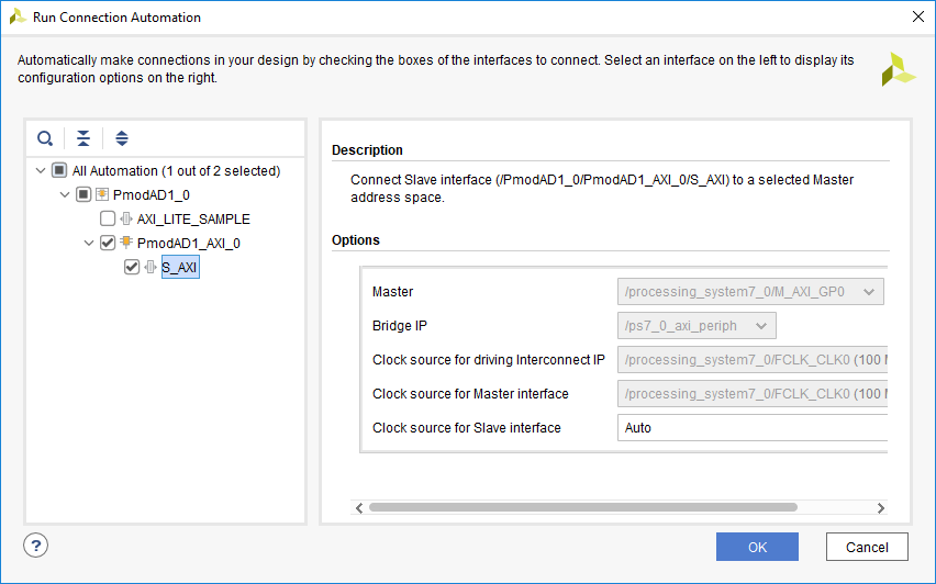
- Connect all of the hierarchical block's AXI interfaces to the processor in the design by clicking on Run Connection Automation, and checking the appropriate boxes. These interfaces may appear more than once in the connection automation dialog. Select only one entry for each interface.
- Connect any interrupts the Hierarchy may have to the appropriate interrupt controller: an AXI Interrupt Controller IP (for Microblaze designs), the Zynq Processing System's irq_f2p port (for Zynq designs).
- Connect any additional clocks to clocks generated by a Memory Interface Generator or a Clocking Wizard (for Microblaze designs), or a Zynq Processing System (for Zynq designs).
5.
The next step, constraining the Hierarchy's Pmod_out port, has two different workflows.
If a board was selected when creating the project, the Board Flow can be used for this step:
- Board Flow
-
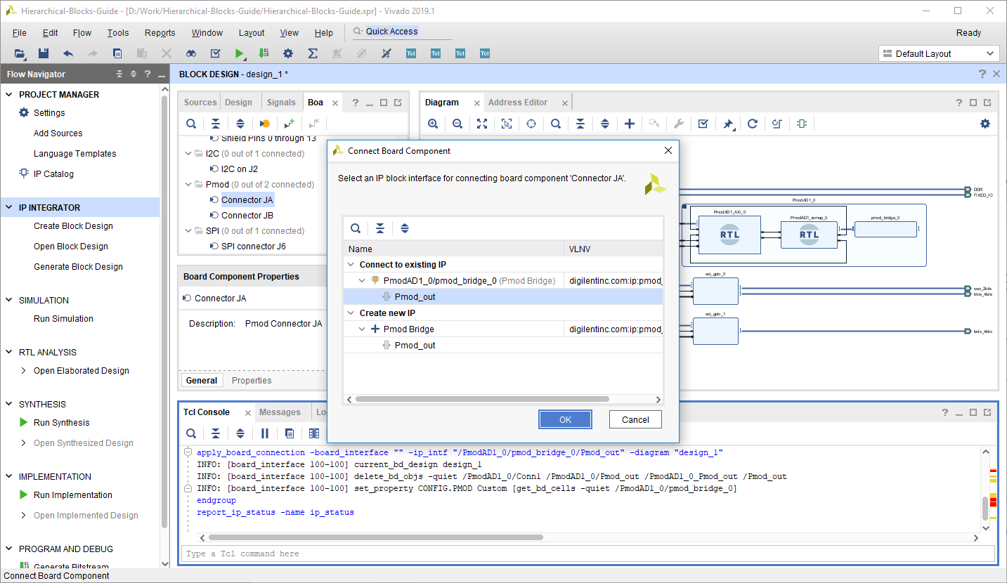
- Go to Vivado's Board tab and select a Pmod connector to connect to the hierarchical block. Right click on the connector's entry, typically named something like “Connector JA”, and select Connect Board Component. In the popup window, under Connect to existing IP, select the “Pmod_out” interface of the Hierarchy's Pmod Bridge IP. Click OK.
- Validate the block design, save it, and create an HDL wrapper file, if one doesn't already exist.
- Check the README.txt file in the hierarchical block's folder in vivado-hierarchies-master for additional instructions to determine whether any additional constraints are required.
If a part was selected instead of a board, or the Board Flow cannot be used for whatever reason, the Hierarchy's Pmod_out port must be made external and its pins must be manually constrained:
- Manual Constraint Flow
-
- Select the Pmod_out port, then right click on it and select Make External. Select the newly created external interface port (named something like “Pmod_out_0”) in the design, and give it a memorable name.
- Validate the block design, save it, and create an HDL wrapper file, if one doesn't already exist.
- When the Hierarchy was created, a constraint file, named “(Default Hierarchy Name)_Pmod_out.xdc”, was imported into the project. This file contains the constraints required when not using the board flow. Uncomment each line starting with “set_property” by removing the leading “#” symbol.
- The text “FIXME” appears in several places in the constraint file. These correspond to places where values, specific to the board and design, must be manually entered.
- Find the correct port names for the Pmod_out interface by reviewing the top module's port map near the top of the HDL wrapper file. Enter these port names into the constraint file, replacing the “FIXME“s after get_ports, near the end of each line.
- Download the master XDC file for the board. Master XDC files for Digilent boards can be found in the digilent-xdc repository on Github. Find the LOC property values that correspond to the Pmod connector that the hierarchical block's Pmod_out port is to be connected to. Enter these values into the corresponding LOC fields in the hierarchy's constraint file.

6.
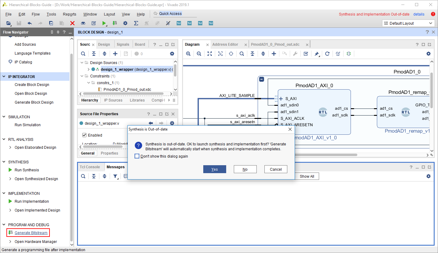
Click Generate Bitstream. This process may take some time, depending on the complexity of the project.
7.
Export the hardware design and bitstream to SDK by selecting File → Export → Export Hardware in the menu bar at the top of the window. In the resulting pop up window, check the Include bitstream box, then click OK.

8.
Launch Xilinx SDK by selecting File → Launch SDK in the menu bar at the top of the window. Make sure to set the <Exported location> to be the same location chosen in Step 7 above.

9.
Create a new application project using the “Empty Application” template. Make sure to check if the hierarchical block requires any changes to project settings or if any libraries must be added to the BSP. These requirements, if any, are detailed in the README.txt file in the Pmod's sdk_sources folder in the vivado-hierarchies-master folder.

10.
Copy all of the files from the selected hierarchical block's sdk_sources folder (in the vivado-hierarchies-master folder), then paste them into the application project's src folder.

12.
Make sure that the development board's programming mode select jumper is set to JTAG. Plug the board into the computer via its microUSB programming port and power it on.
Connect the SDK Terminal to the port associated with the board. The green button in the Serial Terminal pane is used to launch the Connect to a serial port dialog. By default, the baud rate is 115200 for Zynq, and 9600 for Microblaze (when using the AXI Uartlite IP). If desired, other terminals, such as Tera Term or PuTTY, may be used instead.

13.
Program the FPGA by selecting Xilinx → Program FPGA from the top menu bar in Xilinx SDK.
Once the FPGA is programmed, run the application project by right-clicking on the application project and selecting Run → Run on Hardware (System Debugger).
Messages printed by the demo application can be seen in the serial terminal.
