


Editor’s Note – In this series, we will take a behind the scenes look at how an engineer tackles a project from beginning to end. What challenges will come up? How can we face problems and come up with solutions? Aside from project completion, what are successes that we can celebrate along the way?
- Post 1 – Introducing Ryan
- Post 2 – Initial Considerations
- Post 3 – Designing a Zmod Peripheral
- Post 4 – Setting Up SYZYGY DNA
- Post 5 – Writing SYZYGY DNA Using the ADP3450
- Post 6 – Packing an IP in Vivado
- Post 7 – Preparing a Vivado Project
Using the ADP5250 to Test a Design
This entry will be split into two parts. In the first part, we’ll cover the creation of an application project in Vitis, while the second part is a look at how the ADP5250 was used to analyze these signals.
Creating an Application Project in Vitis
The first step is to go to ‘File’ -> ‘New’ -> ‘Application Project’, after clicking on the first ‘next’, the below window should be visible.
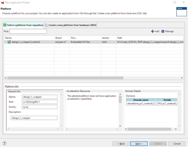
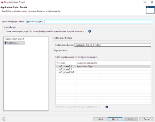
Now we must click on ‘Create a new platform from Hardware (XSA)’. By clicking the browse button, we must select the hardware specification exported from Vivado (previous entry). A project name must be given to the project and the ‘ps7_cortexa9_0’ processor must be selected. Figure 2 illustrates these options in Vitis.
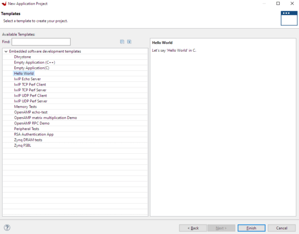
When the below window is visible in Vitis, the ‘Hello World’ project option must be selected so we have this template available.
After this, your Vitis Project Explorer Menu should look like this:
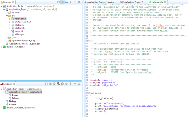
In this project, there is no need to insert any additional C-code for the ARM A9 processor on the SoC since our signals are generated from the programmable logic section (FPGA) of the SoC. All that is left to do now is to load our design into the SoC. After making sure that the Eclypse Z7 is connected to the PC, right click on the application project -> Run As -> Launch Hardware. The program should now be loaded into the SoC onboard the Eclypse. It is now time to test!
Using the ADP5250 to Analyze Signals From the New Zmods
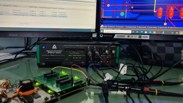
It is quite straightforward to connect the ADP5250 to the I/O ports of the Zmods. I am using the P2150 150MHz BNC probes connected to my outputs. I have connected the probes to the oscilloscope inputs of the ADP5250.
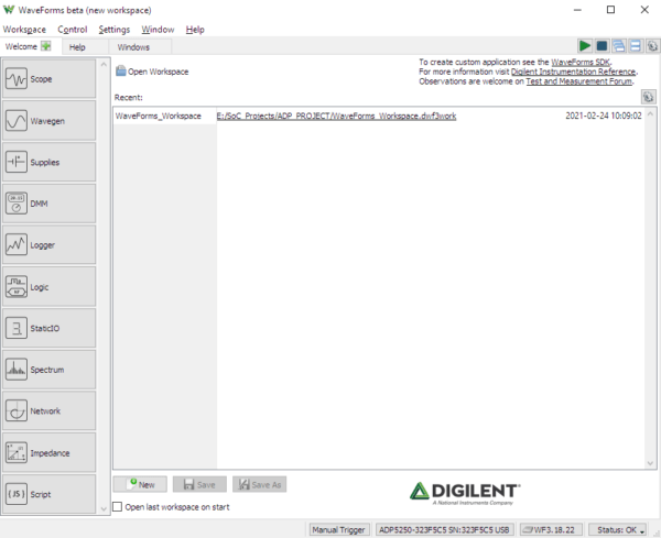
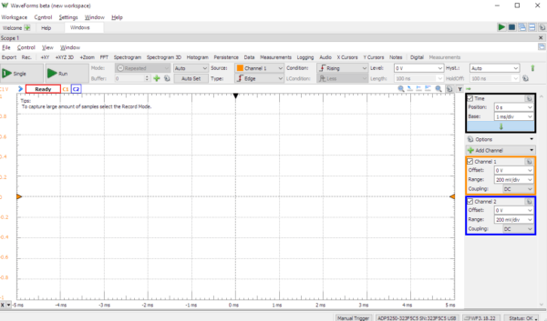
It was actually surprising to experience how simple this process is with Digilent’s software. Once WaveForms is open it will detect the ADP5250 immediately. From WaveForms (figure below), simply click on the Scope tab (top left corner).
Since our output signals range from 0V to 1.8V, it is ideal to set the offset of channel 1 to -2V and the range option of both channels to 500mV/div. This provides a good view of the two signals which we will be testing for.
After pressing the ‘Run’ button on the top left corner of the scope panel in WaveForms, here is our result:
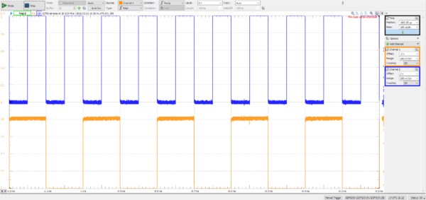
This result is perfectly as expected! One of the signals presents half of the frequency of the other. This is due to the divider setting we applied to the clock divider IP core design and explained in Post 7 – Preparing a Vivado Project.
This was my first time using the ADP5250, and I can say, what an excellent tool! It is simply everything an engineer could ever want on their benchtop! Not only is it compact, it looks great on the bench. I truly wish I had this during my Engineering Degree, it would have made life much easier. In the next entry of Engineers in the Wild, the ADP5250’s various features will be put to good use. See you then!