


Editor’s Note – In this series, we will take a behind the scenes look at how an engineer tackles a project from beginning to end. What challenges will come up? How can we face problems and come up with solutions? Aside from project completion, what are successes that we can celebrate along the way?
In this entry I will be going over the hardware which will be used in the RF Front End board that I’m working on for the series, expected functionality, RF Electronic circuit design considerations, compactness of design, and challenges involved in such a design.
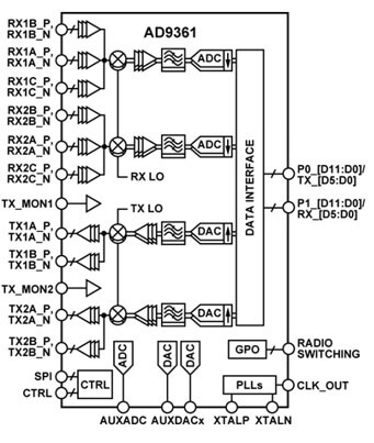
The need for an RF front end chip is critical to design a small, compact, and power efficient wireless transmission daughter board (a circuit board that plugs into and extends the circuitry of another circuit board). The design will incorporate the AD9361, which is a high performance, highly-integrated radio frequency (RF) Agile Transceiver™ from Analog Devices. Packaged in a 10 mm × 10 mm, 144-ball chip scale package ball grid array, the AD9361 combines a RF front end with a flexible mixed-signal baseband section and integrated frequency synthesizers, simplifying design-in by providing a configurable digital interface to a processor. With the ability to operate between 70MHz and 6GHz, the AD9361 is ideal for a wide range of radio frequency applications such as 3G and 4G base stations, making it a very versatile chip and giving us the ability to experiment with various frequencies of transmission and reception of the wireless signals. The chip also provides two transmission ports and two reception ports, which will both be utilized in the design. In fact, one of the transmission outputs will be connected to an RF power amplifier in order to increase the wireless transmission range. The designed board is expected to be able to handle various wireless transmission and reception techniques, which will be used to study the best wireless transmission protocol and frequency for a given application such as audio and video transmission. Figure 1 (below) illustrates the AD9361 functional block diagram, the internal architecture of the chip.
The complete circuit design around the AD9361 incorporates, power supplies with decoupling circuitry, RF differential signal couplers and decouplers, power supply, monitor, analog-to-digital converter (Serial Peripheral Interface SPI), on board EEPROM for data storage (SPI), and other components. An SPI bus will be used to communicate with the RF front end chip (AD9361), EEPROM and analog-to-digital converter.
Design For Electromagnetic Compatibility
Such a circuit presents a number of challenges when migrating from a schematic to a printed circuit board (PCB) design. This is due to physical phenomena related to high frequency signals propagating trough conductors such as copper. When a high frequency signal is propagating through a conductor, a number of effects can be observed such as the conductor behaving similarly to inductors or capacitors or the conductor behaving as an antenna due to internal reflections. In order to rectify these effects as much as possible, impedance matching between devices, conductors and ports is imperative. Additionally, a perfectly matched system will be able to maximize the power transmitted from one point to the other.
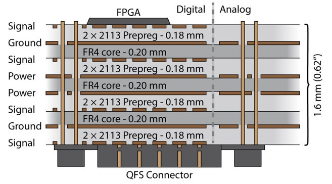
In order to reduce electromagnetic interference, a multilayer PCB with strategically placed ground and power planes is important. Digital signal lines must be buried inside the PCB in between ground and power planes in order to minimize interference. The figure above illustrates an ideal set-up of the PCB’s tracks, which will be used in the implementation of this design. Physically separating RF signal tracks is another important technique to further reduce crosstalk.
Such considerations have to be made by electronics engineers when embarking on new hardware designs in order to reduce as far reasonably practicable future issues with hardware.
In the next entry for “Engineers in the Wild”, I will be discussing the design in terms of the resulting Zmod daughter board, providing details on what one may use such a board for and how communication between the ZYNQ chip on a Digilent board will communicate to the AD9361. See you then!
One Comment on “Engineers in the Wild: Wireless Radio Frequency Circuit Design – Initial Considerations”