

In this post, the hardware design for the Eclypse Z7 to perform wireless communication is discussed. The initial considerations behind the circuit design and PCB design have discussed in this post. The required circuitry and software for conformity with the SYZYGY specification is given here. The design was based around the AD9361 RF Front End Chip from Analog Devices which provides a fully integrated RF Front End which only required a base band processor for setting up and wireless protocol software. The next section describes the required power supply designs for the AD9361.
Power Supplies for the AD9361
The AD9361 Requires two main power supplies, these are a 1.3V power supply for the Analog circuitry inside the chip and a power supply named as VDD_INTERFACE. The VDD_INTERFACE power supply determines the voltage level at which the AD9361 communicates with the baseband processor (BBP), which in this case is the ZYNQ system on chip on the Eclypse Z7. The ZMOD connectors on the Eclypse provide 5V, 3.3V power supplies and a variable supply called VIO. It is important to note that the design makes use of both ZMOD connectors on the Eclypse Z7 which according to the SYZYGY specification is called a double wide POD. A high-level view of the connections of the ZMOD connectors to the rest of the circuitry on the ECLYPSE Z7 and power supplies is illustrated in figure 1. The VIO voltage of the ZMOD has been set to 2.5V, this was done using the SYZYGY DNA data which upon power up is passed to the SYZYGY Controller on the Eclypse which sets this voltage accordingly.
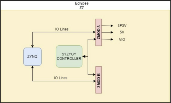
Figure 1: ZMOD connection overview
Low drop out (LDO) regulators have been used in order to drop down the 3.3V supply from the ZMODS to the required 1.3V. Two separate LDOs have been used for two separate 1.3V supplies, this is recommended in the reference manual of the AD9361 in order to minimize the effects of power supply noise on the analog circuitry of the chip. The power supplies provided by the ZMOD ports on the Eclypse make it perfect for a wide range of applications and this was one of the reasons the Eclypse was used in this project.
Digital Interface
The AD9361 is set up by the BBP processor using a Serial Peripheral Interface (SPI) bus, this is used to give the settings to the RF Front end such as the frequency of transmission and reception. Figure 2 illustrates the connections required in Low Voltage Differential Signaling (LVDS) mode between the AD9361 and the ZYNQ on the Eclypse. The differential signals were used due to their improved performance in noisy environments and thus increased reliability in parallel digital communications. The differential signals on the ZMOD connectors of the Eclypse have been used to pass the data to the ZYNQ.

RF Interface
AD9361s RF interfaces are differential and thus RF transformers were used in order to get a single ended signal to connect to the SMA connectors (Antenna Connectors). On one of the RF output ports of the RF front End an amplifier was designed and placed in order to amplify the signal coming out of the AD9361 this has provided the benefit of increased wireless communication range. RF transmission lines have been used in the PCB in order to provide very important impedance matching in RF designs.
PCB Design
Due to the increased complexity of the AD9361 and the high pin count, printed circuit board (PCB) layout is important to get the best performance. The first step undertaken in order to design this PCB was to make decisions with regards to the stack up. The stack up of a PCB is the definition of the layers which are incorporated in a PCB. The main aims for the design with regards to the stack up were:
- Reduction of high frequencies losses in the PCB
- Proper reference ground planes for transmission lines
- Isolating the RF section from digital circuitry
- Impedance control and matching
- Maintaining signal launch integrity
Table 1 below shows the stack up designed for this PCB given the priorities outlined above. The PCB was designed to be 10 layers. This provided layers which can be fully dedicated to ground planes in order to sandwich digital and RF signals between ground layers which reduce digital to RF circuit coupled noise.
| Layer | Layer Usage | Notes |
| Top | RF Traces | 50ohm impedance matched |
| 2 | Ground Reference Plane | Reference for Top RF traces |
| 3 | Power Supplies Layer | Power Planes |
| 4 | Ground Plane | Barrier for Digital Transients |
| 5 | Digital Signals | Differential and Single Ended |
| 6 | Digital Signals | Differential and Single Ended |
| 7 | Ground Plane | Barrier for Digital Transients |
| 8 | Power Supplies Layer | Power Planes |
| 9 | Ground Reference Plane | Reference for Bottom RF traces |
| Bottom | RF Traces | 50ohm impedance matched |
Table 1: Layer allocation of the Designed PCB
The RF traces have been routed on the top and bottom sides of the PCB and some internal layers have been used to route power planes. Figures 3 and 4 show a 3D view of the designed double wide RF Front End ZMOD.
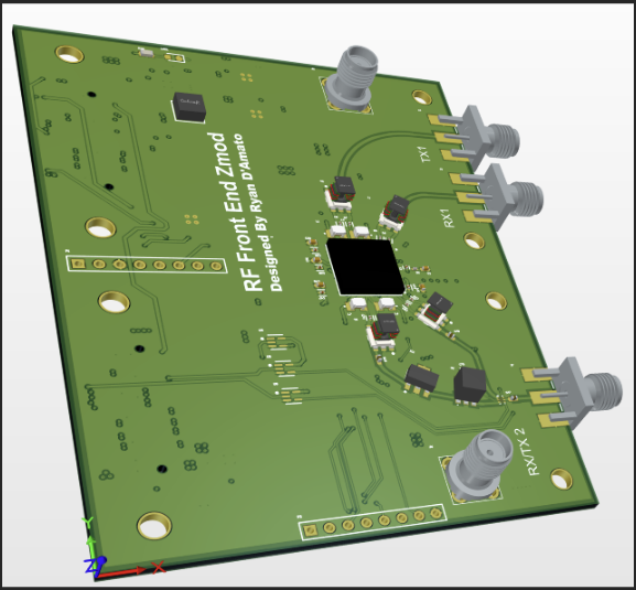
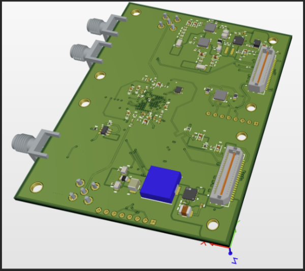
The RF transmission lines of the AD9361 to the SMA connectors are visible on the Top side of the PCB. While all power supply circuitry designed for the AD9361 is visible on the bottom side of the PCB, The ZMOD connectors which fit exactly into the Eclypse are also clearly visible. The reason for putting all the power supply circuitry on the bottom side is to minimize the noise interference power supply circuitry generates to the AD9361. After implementing all the necessary software, the designed hardware was found to function perfectly. In fact the PMOD connectors on the Ecypse Z7 have been used together with a PMOD i2S2 peripheral and wireless audio transmission between two Eclypses has been achieved!!
The power of the Eclypse Z7 in my opinion lies with the availability of both ZMOD and PMOD ports which together with the designed RF Front End ZMOD make up an extremely versatile Software Defined Radio (SDR) due to it being capable of being used with various PMOD peripherals. This could result in wireless transmission of data captured via a PMOD peripheral such as an ADC or any other.