
Editor’s Note – In this series, we will take a behind the scenes look at how an engineer tackles a project from beginning to end. What challenges will come up? How can we face problems and come up with solutions? Aside from project completion, what are successes that we can celebrate along the way?
- Post 1 – Introducing Ryan
- Post 2 – Initial Considerations
- Post 3 – Designing a Zmod Peripheral
- Post 4 – Setting Up SYZYGY DNA
- Post 5 – Writing SYZYGY DNA Using the ADP3450
Packaging an IP in Xilinx’s Vivado
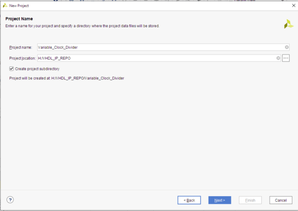
In order to check that all connections between the SoC on the Eclypse and our newly designed Zmods, a test project has to be constructed and loaded into the Eclypse Z7. Some IP sources will be needed to provide the necessary functionality. For this project a simple VHDL clock divider is going to be used in order to output square waves of variable desired frequencies on the outputs. As shown in the figure below, a new Vivado project has been opened in my IP repository folder. Figure 2 illustrates the chosen option, ‘RTL Project’.

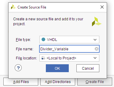
A new VHDL file in the project has been created as shown in the figure below.
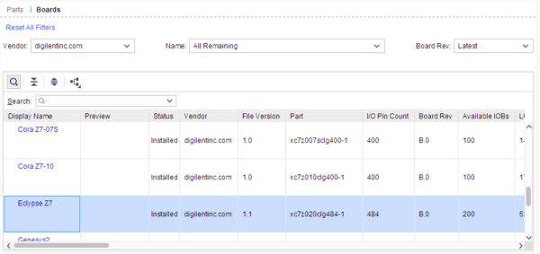
When the window to choose your device pops up, the vendor setting defaults to ‘digilentinc.com’ and the Eclypse Z7 board has been chosen. Make sure you have the Digilent board files installed!
The VHDL code pasted at the end of this post is the VHDL functionality of a clock divider with one clock input and two clock outputs. After the code has been written in the VHDL file created in the Vivado project, from the ‘Tools’ menu in Vivado, ‘Create and package new IP’ option has been chosen. In the pop up window, the ‘Package Your Current Project’ option has been chosen (Figure 5). This will package our Vivado project into an IP!

After selecting the location for packaging the IP, the window illustrated in Figure 6 should appear on your screen.
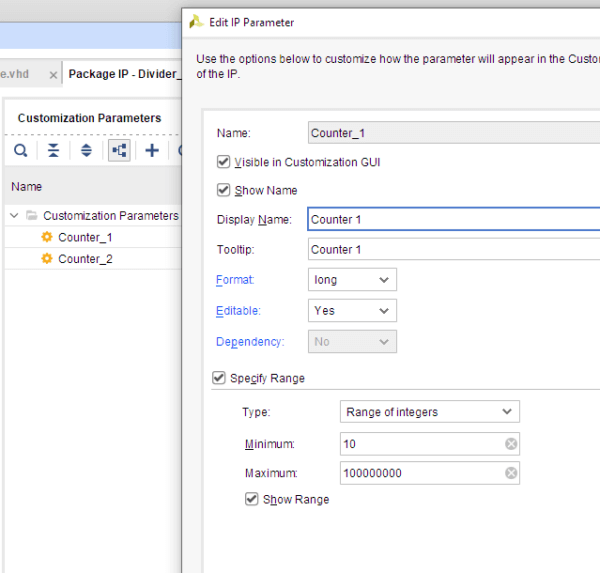
From the ‘Customization Parameters’ tab of the IP Packager, the parameters can be edited. In this case I have put a range value to these parameters as illustrated in the figure below.
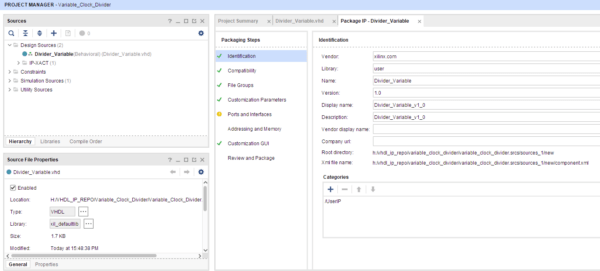
After all has been set, the ‘Package IP’ button has been pressed (Figure 8).
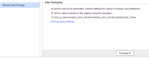
Figures 9 and 10 show how the packaged IP looks in a separate project in Vivado.
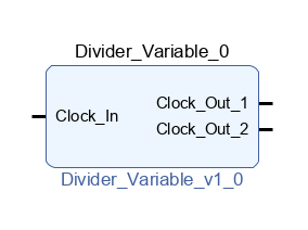
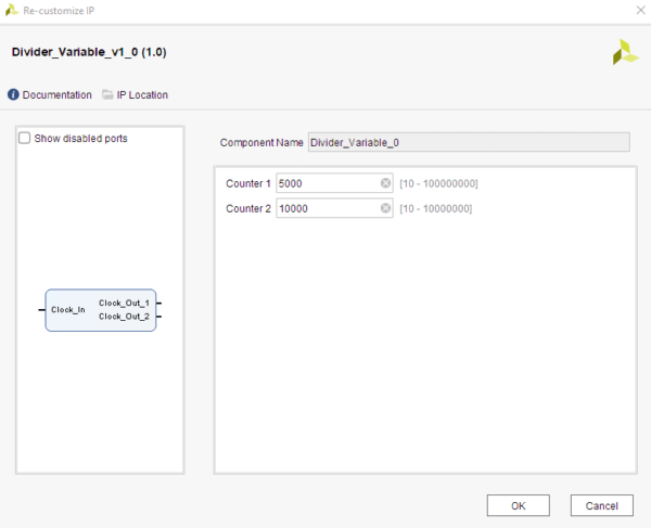
Now the IP has been successfully packaged!
The VHDL divider code basically works by counting the times a positive edge is present on the input clock. When the counters reach the value set by the user, the output clock logic state is inverted. This provides a division of the input clock frequency on the output clock.
library IEEE;
use IEEE.STD_LOGIC_1164.ALL;
use IEEE.numeric_std.ALL;
— Uncomment the following library declaration if using
— arithmetic functions with Signed or Unsigned values
–use IEEE.NUMERIC_STD.ALL;
— Uncomment the following library declaration if instantiating
— any Xilinx leaf cells in this code.
–library UNISIM;
–use UNISIM.VComponents.all;
entity Divider_Variable is
Generic(
Counter_1: INTEGER := 5000;
Counter_2: INTEGER := 10000
);
Port (
Clock_In: in std_logic;
Clock_Out_1: out std_logic;
Clock_Out_2: out std_logic
);
end Divider_Variable;
architecture Behavioral of Divider_Variable is
signal count_1, count_2: integer:=1;
signal tmp_1, tmp_2 : std_logic := ‘0’;
begin
process(Clock_In)
begin
if(Clock_In’event and Clock_In=‘1’) then
count_1 <=count_1+1;
if (count_1 = Counter_1) then
tmp_1 <= NOT tmp_1;
count_1 <= 1;
end if;
end if;
Clock_Out_1 <= tmp_1;
end process;
process(Clock_In)
begin
if(Clock_In’event and Clock_In=‘1’) then
count_2 <=count_2+1;
if (count_2 = Counter_2) then
tmp_2 <= NOT tmp_2;
count_2 <= 1;
end if;
end if;
Clock_Out_2 <= tmp_2;
end process;
end Behavioral;
In the next entry, we will discuss in detail the project which will be used to test the I/Os on the newly designed Zmods.

