This is an old revision of the document!
Pmod OC1 Reference Manual
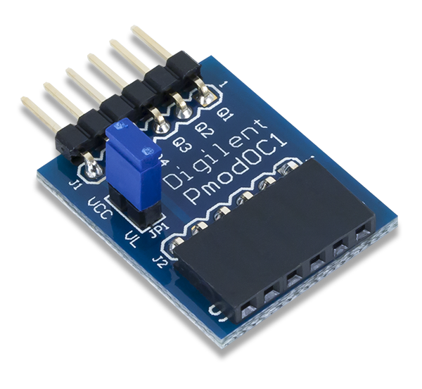
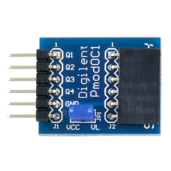
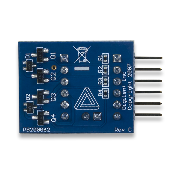
The Digilent Pmod OC1 (Revision C) uses open-collector BJTs to drive high current applications.
Download This Reference Manual
Features
- Four 100mA (200mA max) transistors
- Four output clamp diodes
- 40V voltage threshold
- 6-pin Pmod port with GPIO interface
Functional Description
The Pmod OC1 utilizes MMBT3904 transistors in an open collector format. Each transistor can drive up to 100 mA of current individually and can draw up to 200 mA of current.
Interfacing with the Pmod
The Pmod communicates with the host board via the GPIO protocol. A logic level high voltage will “turn on” the BJT and a logic low signal will keep the BJT “off”.
Pinout Description Table
| Pin | Signal | Description |
|---|---|---|
| 1 | P1 | Output 1 |
| 2 | P2 | Output 2 |
| 3 | P3 | Output 3 |
| 4 | P4 | Output 4 |
| 5 | GND | Power Supply Ground |
| 6 | VCC | Positive Power Supply |
Any external power applied to the Pmod OC1 must be within 2.7V and 5.25V; however, it is recommended that Pmod is operated at 3.3V.
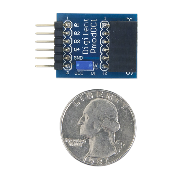
Physical Dimensions
The pins on the pin header are spaced 100 mil apart. The PCB is 1 inch long on the sides parallel to the pins on the pin header and 0.8 inches long on the sides perpendicular to the pin header.
Additional Information
The schematics of the Pmod OC1 are available here. Additional information about the BJTs including specific timings of the chip can be found by checking out its datasheet here.
Example code demonstrating how to get information from the Pmod OC1 can be found here.
If you have any questions or comments about the Pmod OC1, feel free to post them under the appropriate section (“Add-on Boards”) of the Digilent Forum.