This is an old revision of the document!
Getting Started with Zynq

Overview
This guide will provide a step by step walk-through of creating a hardware design using the Vivado IP Integrator for the Zybo board.
At the end of this tutorial you will have:
- Created a simple hardware design incorporating the on board LEDs and switches.
- Created a .C project in XIlinx Vivado SDK tieing the on board LEDs and switches together using the hardware design shown in the previous step.
Prerequisites
Hardware
- Digilent's Zybo Development Board and a Micro USB cable for UART communication and JTAG programming
Software
- Xilinx Vivado 2015.X with the SDK package.
Board Support Files
- Zybo Support Files
- These files will describe GPIO interfaces on your board and make it easier to select your board in the initial design setup and add GPIO IP blocks in the block design
- Follow this Wiki guide Vivado Board Files for Digilent 7-Series FPGA Boards on how to install Board Support Files for Vivado 2015.X
Tutorial
General Design Flow
I. Vivado
- Open Vivado and select Zybo board
- Create an new Vivado Project
- Create empty block design workspace inside the new project
- Add required IP blocks using the IP integrator tool and build Hardware Design
- Validate and save block design
- Create HDL system wrapper
- Run design Synthesis and Implementation
- Generate Bit File
- Export Hardware Design including the generated bit stream file to SDK tool
- Launch SDK
Now the Hardware design is exported to the SDK tool. The Vivado to SDK hand-off is done internally through Vivado. We will use SDK to create a Software application that will use the customized board interface data and FPGA hardware configuration by importing the hardware design information from Vivado.
II. SDK
- Create new application project and select default Hello World template
- Program FPGA and run application
1. Creating a New Project
When you first run Vivado this will be the main start window where you can create a new project or open a recent one.
1.1) Click on Create New Project.

1.2) You will be presented with the project creation wizard. Click Next.

1.3) Enter a project name and location the click Next.

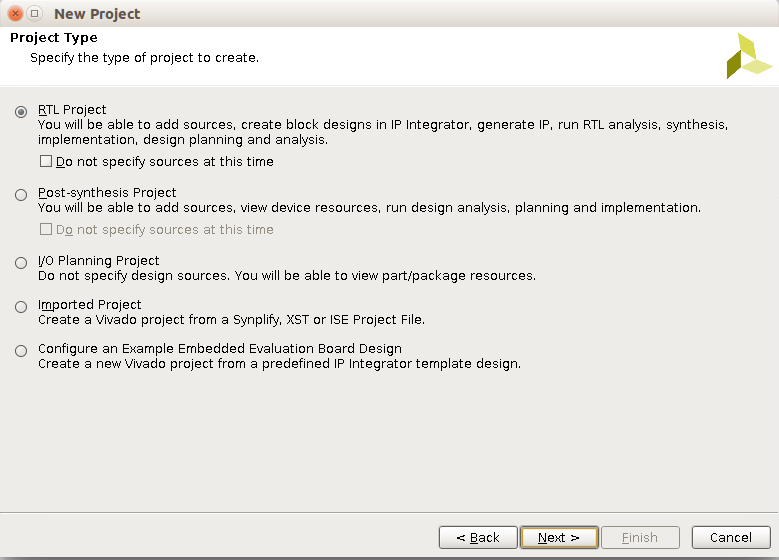
1.4) Select RTL Project and click Next.
1.5) This demo does not use any existing sources, existing IP or constraints. Click through the next three screens.

1.6) Select Boards and select the Zybo board file. Click Next and then Finish.

2. Creating a New Block Design
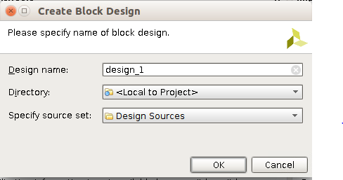
2.1) Once the process has completed, click Create Block Design in the flow navigator.

2.2) Click OK.
2.3) A blank Block Design will open up.
3. Add the Zynq IP & GPIO Blocks
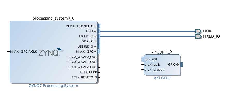
3.1) Click theAdd IP button and search for ZYNQ. Double click on ZYNQ7 Processing System to place the bare Zynq block.

3.2) Click the Run Block Automation link
Your Zynq block should now look like the picture below.


3.3) Click the
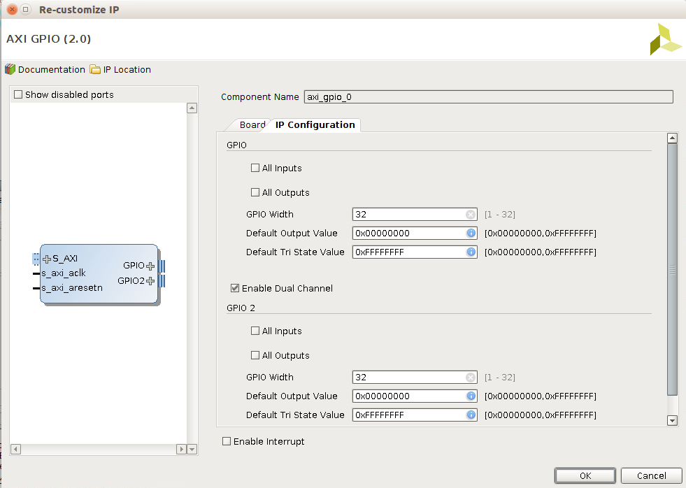
3.4) Double-click on new axi_gpio_0 core that was just added to bring up the customizing window. Under the IP Configuration tab check the Enable Dual Channel box. Click OK.
3.5) Add another GPIO core by repeating step 3.4 but do not enable dual channel.

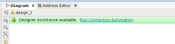
4. Run the Connection Automation Tool
4.1) The connection automation tool will add the required logic blocks for the demo. Select Run Connection Automation highlighted in blue.
4.2) Check the box by All Automation. Select GPIO under axi_gpio_0 and select btns_4bits in the Board Part Interface drop-down box.

4.3) Select GPIO2 under axi_gpio_0 and select swts_4bits in the drop-down box.

4.4) Select GPIO under axi_gpio_1 and select leds_4bits in the drop-down box and hit OK.
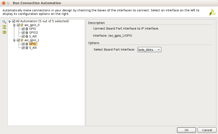
4.5) This process will add:* The AXI interconnect * Processor System Reset * The board parts for the buttons, switches and LEDs.
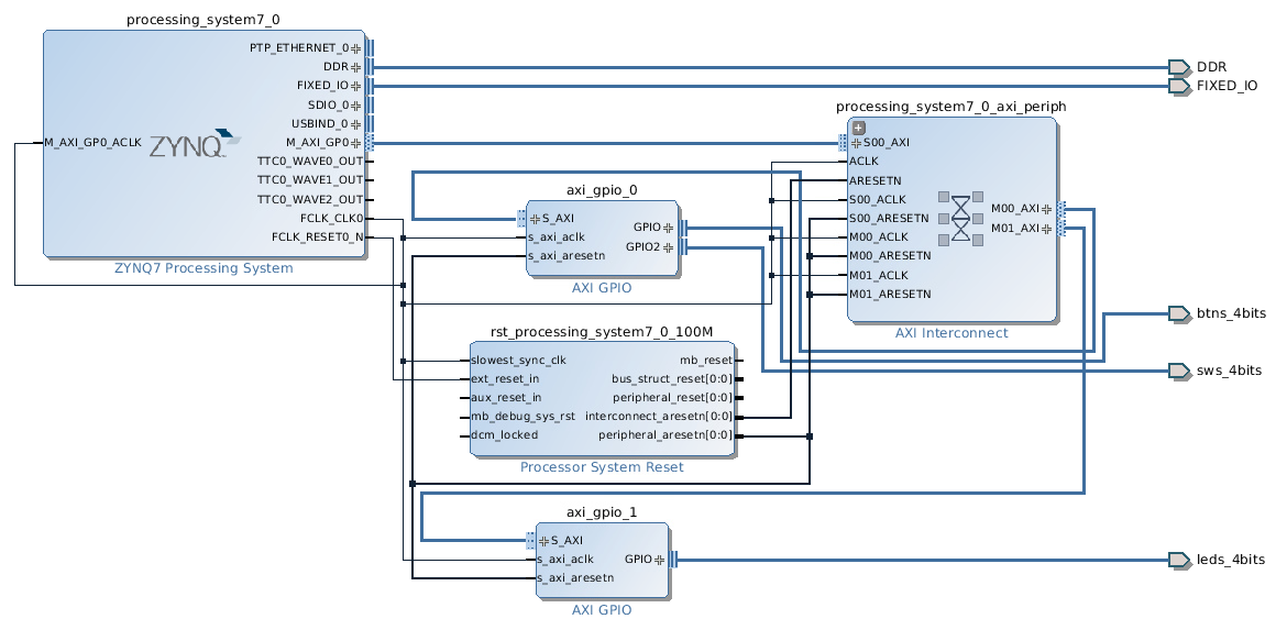
4.6) Next let's clean up our Block Design. Click theRegenerate Layout button to rearrange your block design.

5. Generate HDL Wrapper and Validate Design
5.1) SelectValidate Design. This will check for design and connection errors.
5.2) After the design validation step we will proceed with creating a HDL System Wrapper. In the block design window, under the Design Sources tab, right-click on the block diagram file. We labeled it “design_1.bd” and select Create HDL Wrapper.

This will create a top module in VHDL and will allow you to generate a bitstream.
6. Generate the Bitstream
6.1) Click on Generate Bitstream at the bottom of the Flow Navigator. Wait for the process to complete and click OK.

7. Export hardware files for SDK
7.1) Go to file→Export→Export Hardware… Make sure to check the box for Include bitstream then click OK.

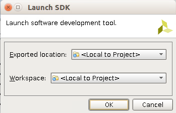
8. Launch SDK
8.1) Go to File→Launch SDK and click OK.
9. Create a new Hello World Application Project
9.1) Go to File→New→Application Project.

9.2) Enter the project details:* Project name: "getting_started_with_ZYBO" * Hardware Platform: design_1_weapper_he_platform_0 * Processor: ps7_cortexas9_0 * Languate: C * OS Platform: standalone * Board Support Package: Create New (leave default name)

9.3) The Hello World demo is a good starting point for this demo. Click Next, select Hello World and click Finish. This process will add two directories to the project explorer.
9.4) Expand getting_started_with_ZYBO then open src and double click on “helloworld.c”. This is the default Hello World C code.

10. Creating Our Own Hello World
10.1) Copy and paste the code below into the helloworld.c file.
/*****************************************************
Getting Started Guide for Zybo

This demo displays the status of the switches on the
LEDs and prints a message to the serial communication
when a button is pressed.

Terminal Settings:
   -Baud: 115200
   -Data bits: 8
   -Parity: no
   -Stop bits: 1

1/6/14: Created by MarshallW
****************************************************/

#include <stdio.h>
#include "platform.h"
#include <xgpio.h>
#include "xparameters.h"
#include "sleep.h"

int main()
{
   XGpio input, output;
   int button_data = 0;
   int switch_data = 0;

   XGpio_Initialize(&input, XPAR_AXI_GPIO_0_DEVICE_ID);	//initialize input XGpio variable
   XGpio_Initialize(&output, XPAR_AXI_GPIO_1_DEVICE_ID);	//initialize output XGpio variable

   XGpio_SetDataDirection(&input, 1, 0xF);			//set first channel tristate buffer to input
   XGpio_SetDataDirection(&input, 2, 0xF);			//set second channel tristate buffer to input

   XGpio_SetDataDirection(&output, 1, 0x0);		//set first channel tristate buffer to output

   init_platform();

   while(1){
      switch_data = XGpio_DiscreteRead(&input, 2);	//get switch data

      XGpio_DiscreteWrite(&output, 1, switch_data);	//write switch data to the LEDs

      button_data = XGpio_DiscreteRead(&input, 1);	//get button data

      //print message dependent on whether one or more buttons are pressed
      if(button_data == 0b0000){} //do nothing

      else if(button_data == 0b0001)
         xil_printf("button 0 pressed\n\r");

      else if(button_data == 0b0010)
         xil_printf("button 1 pressed\n\r");

      else if(button_data == 0b0100)
         xil_printf("button 2 pressed\n\r");

      else if(button_data == 0b1000)
         xil_printf("button 3 pressed\n\r");

      else
         xil_printf("multiple buttons pressed\n\r");

      usleep(200000);			//delay

   }
   cleanup_platform();
   return 0;
}
11. Run the Project
11.1) Make sure that the Zybo is connected to the host PC via the UART USB Port and that JP5 is set to JTAG. To program the FPGA, on the top toolbar, click theProgram FPGA button.
11.2) Save the project. The project will automatically build.
11.3) Expand the getting_started_with_ZYBO directory and the Binaries directory. Right click getting_started_with_ZYBO.elf, and select Run As→Launch on Hardware(GDB).
11.4) The demo will be running on the ZYBO. Try playing around with the 4 switches. Doing so should light its respective LED. Also over the serial port, each button press will produce the message “button x pressed”