This is an old revision of the document!
How To Store Your SDK Project in SPI Flash
Overview
This guide will show you how to easily store your Microblaze/SDK project in the SPI Flash on your 7 series device. Storing a program in Flash allows you to preserve your project through power cycles.
Prerequisites
This guide requires the existence of a Vivado project containing a Microblaze system built complete with Quad SPI, External Memory, and Uart cores, and that you have the appropriate QSPI mode jumper setting on the board. You can follow the steps presented in the Microblaze tutorial, and see below the missing steps for adding QSPI Flash and perform all the connections. Since there are slight differences in the Vivado 2019.1 and the version in which the Microblaze tutorial was created, the user needs to check all the connections in the block design to make sure that are correctly made or present.
Hardware
- Digilent Nexys 4 DDR FPGA Board and Micro USB Cable for UART communication and JTAG programming
Software
- Xilinx Vivado 2019.1 with the SDK package.
Board Support Files
- Board Support Files
- These files will describe GPIO interfaces on your board and make it easier to select your FPGA board and add GPIO IP blocks
- Follow this Wiki guide (Vivado Board Files for Digilent 7-Series FPGA Boards ) on how to install Board Support Files for Vivado
Tutorial
Vivado Steps for creating the block design and generate bitstream
1. Create new project and block design
Follow the steps 1 - 3 of the above mentioned Microblaze tutorial to create a new Vivado project, RTL design and Block design, add Microblaze core.
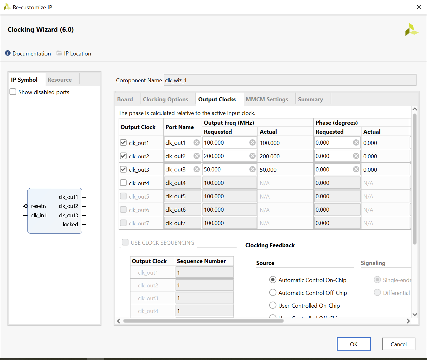
2. Customize Clock Wizard IP Block
Step 4 of the tutorial needs to be modified so it has a new slower Clock of 50MHz, see the picture:
3. Resume steps at 5 from Microblaze tutorial
Add UARTLite IP block, leave the default settings for now, do not perform connection automation
4. Add AXI Quad SPI IP
With the following customization: Mode - Quad, Spansion slave device
5. Run connection automation and regenerate layout
6. Perform some manual connections/check the connections
- Connect the Clocking Wizard “clk_out3” (50Mhz clock) to the “ext_spi_clk” pin.
- Check if the “clk_out1” (100Mhz clock) is connected to the “s_axi_aclk” pin
- Check if the Processor System Reset output port “peripheral_aresetn” is connected to the “s_axi_aresetn” inputs of UARTLite and QSPI blocks
7. Go to step 8 and 9 of the Microblaze Tutorial
The tutorial presents the adding and customization of the Memory Interface Generator IP Block. This step should also contain a customization of the block. Connect the clocking wizard “clk_out2” (200 MHz) clock to “sys_clk_i” of the Ram controller. Run connection automation. Right click the DDR controller “DDR2” pin and make it external. Customizing the MIG interface is not necessarily needed, double click on the module will open a series of pages with default settings, no need for change those.
8. Regenerate layout and validate design
The result should look like in the below image representing the Block Diagram:
9. Create HDL wrapper
10. Synthesize
open the synthesized design, and under I/O Ports tab below the page, check the name of the signals to be written in the XDC file.
11. Create an XDC file and add the constraints in it
You can copy paste the syntax from the Master XDC file for Nexys4DDR
- XDC File signals
-
## This file is a general .xdc for the Nexys4 DDR Rev. C
## To use it in a project:
## - uncomment the lines corresponding to used pins
## - rename the used ports (in each line, after get_ports) according to the top level signal names in the project
## Clock signal
set_property -dict { PACKAGE_PIN E3 IOSTANDARD LVCMOS33 } [get_ports { sys_clock }]; #IO_L12P_T1_MRCC_35 Sch=clk100mhz
create_clock -add -name sys_clk_pin -period 10.00 -waveform {0 5} [get_ports {sys_clock}];
set_property -dict {PACKAGE_PIN C12 IOSTANDARD LVCMOS33} [get_ports {reset}]
#compress bit file
set_property BITSTREAM.GENERAL.COMPRESS TRUE [current_design]
#QSPI signals
set_property -dict {PACKAGE_PIN K17 IOSTANDARD LVCMOS33} [get_ports {qspi_flash_io0_io}]
set_property -dict {PACKAGE_PIN K18 IOSTANDARD LVCMOS33} [get_ports {qspi_flash_io1_io}]
set_property -dict {PACKAGE_PIN L14 IOSTANDARD LVCMOS33} [get_ports {qspi_flash_io2_io}]
set_property -dict {PACKAGE_PIN M14 IOSTANDARD LVCMOS33} [get_ports {qspi_flash_io3_io}]
set_property -dict {PACKAGE_PIN L13 IOSTANDARD LVCMOS33} [get_ports {qspi_flash_ss_io}]
#USB-UART signals
set_property -dict {PACKAGE_PIN D4 IOSTANDARD LVCMOS33} [get_ports {usb_uart_txd}]
set_property -dict {PACKAGE_PIN C4 IOSTANDARD LVCMOS33} [get_ports {usb_uart_rxd}]
#DDR2 Memory signals
set_property -dict {PACKAGE_PIN R7 IOSTANDARD SSTL18_II} [get_ports {DDR2_0_dq[0]}]
set_property -dict {PACKAGE_PIN V6 IOSTANDARD SSTL18_II} [get_ports {DDR2_0_dq[1]}]
set_property -dict {PACKAGE_PIN R8 IOSTANDARD SSTL18_II} [get_ports {DDR2_0_dq[2]}]
set_property -dict {PACKAGE_PIN U7 IOSTANDARD SSTL18_II} [get_ports {DDR2_0_dq[3]}]
set_property -dict {PACKAGE_PIN V7 IOSTANDARD SSTL18_II} [get_ports {DDR2_0_dq[4]}]
set_property -dict {PACKAGE_PIN R6 IOSTANDARD SSTL18_II} [get_ports {DDR2_0_dq[5]}]
set_property -dict {PACKAGE_PIN U6 IOSTANDARD SSTL18_II} [get_ports {DDR2_0_dq[6]}]
set_property -dict {PACKAGE_PIN R5 IOSTANDARD SSTL18_II} [get_ports {DDR2_0_dq[7]}]
set_property -dict {PACKAGE_PIN T5 IOSTANDARD SSTL18_II} [get_ports {DDR2_0_dq[8]}]
set_property -dict {PACKAGE_PIN U3 IOSTANDARD SSTL18_II} [get_ports {DDR2_0_dq[9]}]
set_property -dict {PACKAGE_PIN V5 IOSTANDARD SSTL18_II} [get_ports {DDR2_0_dq[10]}]
set_property -dict {PACKAGE_PIN U4 IOSTANDARD SSTL18_II} [get_ports {DDR2_0_dq[11]}]
set_property -dict {PACKAGE_PIN V4 IOSTANDARD SSTL18_II} [get_ports {DDR2_0_dq[12]}]
set_property -dict {PACKAGE_PIN T4 IOSTANDARD SSTL18_II} [get_ports {DDR2_0_dq[13]}]
set_property -dict {PACKAGE_PIN V1 IOSTANDARD SSTL18_II} [get_ports {DDR2_0_dq[14]}]
set_property -dict {PACKAGE_PIN T3 IOSTANDARD SSTL18_II} [get_ports {DDR2_0_dq[15]}]
set_property -dict {PACKAGE_PIN T6 IOSTANDARD SSTL18_II} [get_ports {DDR2_0_dm[0]}]
set_property -dict {PACKAGE_PIN U1 IOSTANDARD SSTL18_II} [get_ports {DDR2_0_dm[1]}]
set_property -dict {PACKAGE_PIN U9 IOSTANDARD DIFF_SSTL18_II} [get_ports {DDR2_0_dqs_p[0]}]
set_property -dict {PACKAGE_PIN V9 IOSTANDARD DIFF_SSTL18_II} [get_ports {DDR2_0_dqs_n[0]}]
set_property -dict {PACKAGE_PIN U2 IOSTANDARD DIFF_SSTL18_II} [get_ports {DDR2_0_dqs_p[1]}]
set_property -dict {PACKAGE_PIN V2 IOSTANDARD DIFF_SSTL18_II} [get_ports {DDR2_0_dqs_n[1]}]
set_property -dict {PACKAGE_PIN N6 IOSTANDARD SSTL18_II} [get_ports {DDR2_0_addr[12]}]
set_property -dict {PACKAGE_PIN K5 IOSTANDARD SSTL18_II} [get_ports {DDR2_0_addr[11]}]
set_property -dict {PACKAGE_PIN R2 IOSTANDARD SSTL18_II} [get_ports {DDR2_0_addr[10]}]
set_property -dict {PACKAGE_PIN N5 IOSTANDARD SSTL18_II} [get_ports {DDR2_0_addr[9]}]
set_property -dict {PACKAGE_PIN L4 IOSTANDARD SSTL18_II} [get_ports {DDR2_0_addr[8]}]
set_property -dict {PACKAGE_PIN N1 IOSTANDARD SSTL18_II} [get_ports {DDR2_0_addr[7]}]
set_property -dict {PACKAGE_PIN M2 IOSTANDARD SSTL18_II} [get_ports {DDR2_0_addr[6]}]
set_property -dict {PACKAGE_PIN P5 IOSTANDARD SSTL18_II} [get_ports {DDR2_0_addr[5]}]
set_property -dict {PACKAGE_PIN L3 IOSTANDARD SSTL18_II} [get_ports {DDR2_0_addr[4]}]
set_property -dict {PACKAGE_PIN T1 IOSTANDARD SSTL18_II} [get_ports {DDR2_0_addr[3]}]
set_property -dict {PACKAGE_PIN M6 IOSTANDARD SSTL18_II} [get_ports {DDR2_0_addr[2]}]
set_property -dict {PACKAGE_PIN P4 IOSTANDARD SSTL18_II} [get_ports {DDR2_0_addr[1]}]
set_property -dict {PACKAGE_PIN M4 IOSTANDARD SSTL18_II} [get_ports {DDR2_0_addr[0]}]
set_property -dict {PACKAGE_PIN R1 IOSTANDARD SSTL18_II} [get_ports {DDR2_0_ba[2]}]
set_property -dict {PACKAGE_PIN P3 IOSTANDARD SSTL18_II} [get_ports {DDR2_0_ba[1]}]
set_property -dict {PACKAGE_PIN P2 IOSTANDARD SSTL18_II} [get_ports {DDR2_0_ba[0]}]
set_property -dict {PACKAGE_PIN L6 IOSTANDARD DIFF_SSTL18_II} [get_ports {DDR2_0_ck_p[0]}]
set_property -dict {PACKAGE_PIN L5 IOSTANDARD DIFF_SSTL18_II} [get_ports {DDR2_0_ck_n[0]}]
set_property -dict {PACKAGE_PIN N4 IOSTANDARD SSTL18_II} [get_ports DDR2_0_ras_n]
set_property -dict {PACKAGE_PIN L1 IOSTANDARD SSTL18_II} [get_ports DDR2_0_cas_n]
set_property -dict {PACKAGE_PIN N2 IOSTANDARD SSTL18_II} [get_ports DDR2_0_we_n]
set_property -dict {PACKAGE_PIN M1 IOSTANDARD SSTL18_II} [get_ports {DDR2_0_cke[0]}]
set_property -dict {PACKAGE_PIN M3 IOSTANDARD SSTL18_II} [get_ports {DDR2_0_odt[0]}]
set_property -dict {PACKAGE_PIN K6 IOSTANDARD SSTL18_II} [get_ports {DDR2_0_cs_n[0]}]
12. Compress Bitstream (Optional)
In certain applications (often when using the Cmod A7 with Microblaze) you might find that you do not have the necessary space in flash in order to store both your program and bitstream configuration. If this is the case it would be worth a try to compress your bitstream in order to get it to fit. Note that using a compressed bitstream in flash will not only take up less space but will also improve initial FPGA programming speeds. These steps take place in Vivado before the bitstream gets generated.
- With your design ready to be generated into a bitstream select
 from the Flow Navigator.
- Once the implementation has completed either open the implemented design from the pop up window with radio buttons or select
 from the Flow Navigator. The resulting window should look similar to the following:
- With the Implemented Design still on screen select
 and the bitstream settings should pop up.
- Inside of the Bitstream settings check the -bin_file box.

- Next click on Configure additional bitstream settings highlighted in blue at the top of the window. On the following window change the property Enable Bitstream Compresssion to TRUE then select OK until both windows are closed.

- Now Vivado has been configured to output a compressed bitstream which will transfer to your SDK project. Select
 and a window might pop up asking you to save your XDC. If so, give the XDC a name and save it. Your bitstream should start generating afterwards.
13. Export Hardware Handoff
From File→Export→Export Hardware, make sure to check “Include bitstream” setting:

SDK Steps to create a bootloader and program the board
1. Create a SPI Bootloader Application
- To create our bootloader, go to File > New > Application Project.
Name the bootloader then hit Next.
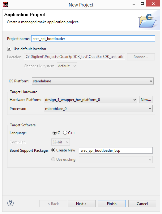
- Select SREC SPI Bootloader and select Finish.

- In your newly created bootloader application, open blconfig.h located in src's and change FLASH_IMAGE_BASEADDR to suit your needs.
It is important to note that this value is the offset that the image will have in Flash. NOTE: If you are using the Cmod-A7 try the offset: 0x00300000.
NOTE: If you are using the Nexys 4 DDR or Arty-A7-100T try the offset: 0x003D0900.
NOTE: If you are using the Arty-A7-35T, Nexys Video or the Genesys 2 try the offset: 0x00C00000.

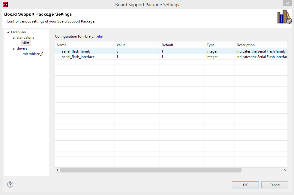
- Next we need to update the BSP to use the updated version of xilisf. To do this, right click on the BSP and select Board Support Package settings and make sure that xilisf is checked and that your version is >= 5.2.

- The memory device info needs to be passed to the xilifs library (Overview > standalone > xilifs).
- serial_flash_family = 5(Spansion/Micron)
- serial_flash_interface = 1(AXI SPI)
- In order to increase the speed even further we can shorten and silence our bootloader. To do this navigate to srec_spi_bootloader > src > bootloader.c, scroll down to where the preprocessor directive VERBOSE is declared and comment it out.

Make sure to re-build the application after making these changes.
2. Create A User Application
This application will be the one that gets stored into Flash. For this tutorial we will be creating a simple Hello World project but the process applies to any project that you would want stored in flash.
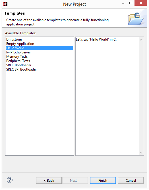
2.1) Create a Hello World application. File > New > Application Project and name your app. Then select Next.

2.2) Select the Hello World application template.
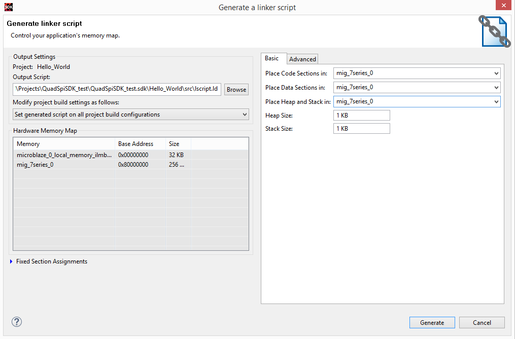
2.3) Next we need to make sure to store our program in DDR. In order to do this, right click on the Hello World application, and select Generate Linker Script.
Place all sections into DDR:
3. Generate Bitstream with BRAM initialized with bootloader
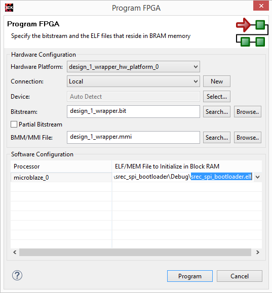
3.1) Open Program FPGA (Xilinx Tools > Program FPGA) and select the bootloader ELF (created in 1.1) under ELF/MEM File to Initialize in block RAM, and select Program to continue.
This will run update_mem, and will output a download.bit file.
4. Program Flash
In this step we will use the SDK Program Flash Memory utility to program our Hello World application to Flash.
4.1) Go to Xilinx Tools > Program Flash. Change the Offset to the value used in blconfig.h in step 1.3.
Select your Flash Type and hit Program.
tip box
For Vivado 2017.1 to the current version of vivado the Arty flash type is mt25ql128-spi-x1_x2_x4

4.2) The Program Flash Memory utility will be used again to store the bitstream initialized with the bootloader in BRAM.
The Image File is the download.bit that was generated in 3.1, and should be located inside of your hardware platform folder.The Offset is 0x0 since the bitstream will be loading our project into memory. Select Program to continue.

5. Test
The flash has now been programmed with our Hello World, SREC, bitstream, and bootloader. With your board connected to a serial port reset the board. This will configure the FPGA and run our Hello World application!