This is an old revision of the document!
Overview
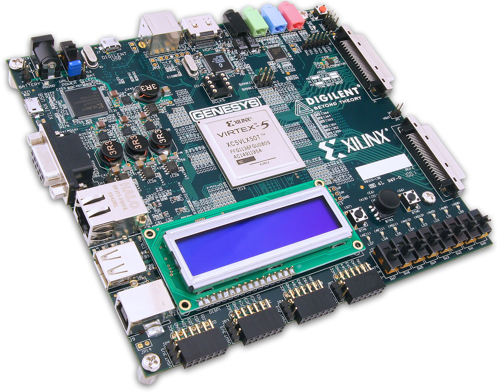
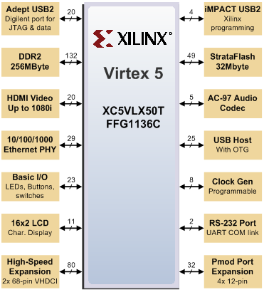
The Genesys circuit board is a complete, ready-to-use digital circuit development platform based on a Xilinx Virtex 5 LX50T. The large on-board collection of high-end peripherals, including Gbit Ethernet, HDMI Video, 64-bit DDR2 memory array, and audio and USB ports make the Genesys board an ideal host for complete digital systems, including embedded processor designs based on Xilinx’s MicroBlaze. Genesys is compatible with all Xilinx CAD tools, including ChipScope, EDK, and the free WebPack, so designs can be completed at no extra cost.
The Virtex5-LX50T is optimized for high-performance logic and offers:
- 7,200 slices, each containing four 6-input LUTs and eight flip-flops
- 1.7Mbits of fast block RAM
- 12 digital clock managers
- six phase-locked loops
- 48 DSP slices
- 500MHz+ clock speeds
The Genesys board includes Digilent's newest Adept USB2 system, which offers device programming, real-time power supply monitoring, automated board tests, virtual I/O, and simplified user-data transfer facilities. A second USB programming port, based on the Xilinx programming cable, is also built into the board.
A comprehensive collection of board support IP and reference designs, and a large collection of add-on boards are available on the Digilent website. See the Genesys page at www.digilentinc.com for more information.
Features
- Xilinx Virtex 5 LX50T FPGA, 1136-pin BGA package
- 256Mbyte DDR2 SODIMM with 64-bit wide data
- 10/100/1000 Ethernet PHY and RS-232 serial port
- multiple USB2 ports for programming, data, and hosting
- HDMI video up to 1600×1200 and 24-bit color
- AC-97 Codec with line-in, line-out, mic, and headphone
- real-time power monitors on all power rails
- 16Mbyte StrataFlash™ for configuration and data storage
- Programmable clocks up to 400MHz
- 112 I/O’s routed to expansion connectors
- GPIO includes eight LEDs, two buttons, two-axis navigation switch, eight slide switches, and a 16×2 character LCD
- ships with a 20W power supply and USB cable
Configuration
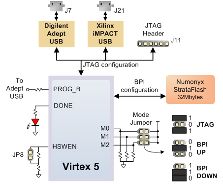
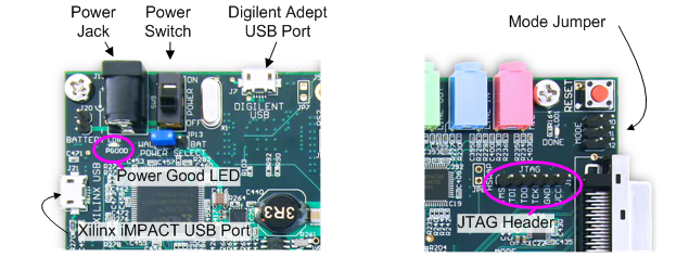
After power-on, the FPGA on the Genesys board must be configured (or programmed) before it can perform any functions. A USB-connected PC can configure the board using the JTAG interface anytime power is on, or a file can be automatically transferred from the StrataFlash ROM at power-on. An on-board “mode” jumper selects which programming mode will be used.
Both Digilent and Xilinx freely distribute software that can be used to program the FPGA and the Flash ROM. Configuration files stored in the ROM use the Byte Peripheral Interface (BPI) mode. In BPI UP mode, the FPGA loads configuration data from the StrataFlash in an ascending direction starting at address 000000. In BPI DOWN mode, configuration data loads in a descending direction starting at address 03FFFF.
Once transferred, programming files are stored in SRAM-based memory cells within the FPGA. These SRAM cells define the FPGA’s logic functions and circuit connections until they are erased, either by removing power or asserting the PROG_B input.
FPGA configuration files transferred using the JTAG interface use the .bin and .svf file types, and BPI files use the .bit, .bin, and .mcs file types. Xilinx’s ISE WebPack and EDK software can create .bit, .svf, .bin, or .mcs files from VHDL, Verilog, or schematic-based source files (EDK is used for MicroBlaze™ embedded processor-based designs). Digilent's Adept software and Xilinx's iMPACT software can be used to program the Genesys board from a PC's USB port.
During FPGA programming, a .bit or .svf file is transferred from the PC to the FPGA using the USB-JTAG port. When programming the ROM, a .bit, .bin, or .mcs file is transferred to the ROM in a two-step process. First, the FPGA is programmed with a circuit that can transfer data from the USB-JTAG port into the ROM, and then data is transferred to the ROM via the FPGA circuit (this complexity is hidden and a simple “program ROM” interface is shown). After the ROM has been programmed, it can automatically configure the FPGA at a subsequent power-on or reset event if the Mode jumpers are set to the proper BPI mode. A programming file stored in the StrataFlash ROM will remain until it is overwritten, regardless of power-cycle events.
Adept System
Adept and iMPACT USB Ports
The Genesys board includes two USB peripheral ports – one for Adept software and another for Xilinx's iMPACT software. Either port can program the FPGA and StrataFlash, but Adept offers a simplified user interface and many additional features such as automated board test and user-data transfers. The Adept port is also compatible with iMPACT, if the Digilent Plug-In for Xilinx Tools is installed on the host PC (download it free from the Digilent website).
The plug-in automatically translates iMPACT-generated JTAG commands into formats compatible with the Digilent USB port, providing a seamless programming experience without leaving the Xilinx tool environment. All Xilinx tools (iMPACT, ChipScope, EDK, etc.) can work with the plug-in, and they can be used in conjunction with Adept tools (like the power supply monitor).
Adept’s high-speed USB2 system can be used to program the FPGA and ROM, run automated board tests, monitor the four main board power supplies, add PC-based virtual I/O devices (like buttons, switches, and LEDs) to FPGA designs, and exchange register-based and file-based data with the FPGA. Adept automatically recognizes the Genesys board and presents a graphical interface with tabs for each of these applications. Adept also includes public APIs/DLLs so that users can write applications to exchange data with the Genesys board at up to 38Mbytes/sec. The Adept application, an SDK, and reference materials are freely downloadable from the Digilent website.
The Xilinx USB port is based on the Xilinx USB programming cable. It can be accessed by all Xilinx CAD tools and iMPACT.
Adept System
Programming Interface
To program the Genesys board using Adept, first set up the board and initialize the software:
- plug in and attach the power supply
- plug in the USB cable to the PC and to the USB port on the board
- start the Adept software
- turn on Genesys' power switch
- wait for the FPGA to be recognized.
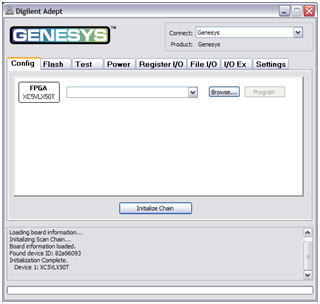
Use the browse function to associate the desired .bit or .svf file with the FPGA, and click on the Program button. The configuration file will be sent to the FPGA, and a dialog box will indicate whether programming was successful. The configuration “done” LED will light after the FPGA has been successfully configured.
Before starting the programming sequence, Adept ensures that any selected configuration file contains the correct FPGA ID code – this prevents incorrect .bit files from being sent to the FPGA.
In addition to the navigation bar and browse and program buttons, the Config interface provides an Initialize Chain button, console window, and status bar. The Initialize Chain button is useful if USB communications with the board have been interrupted. The console window displays current status, and the status bar shows real-time progress when downloading a configuration file.
Flash Interface
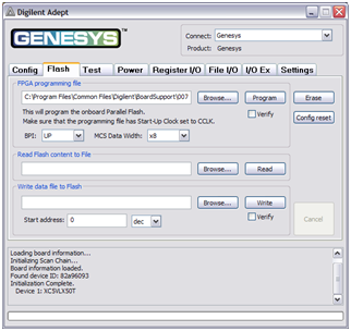
The Flash programming application allows .bin, .bit, and .mcs configuration files to be transferred to the on-board StrataFlash ROM for BPI programming, and allows user data files to be transferred to/from the Flash at user-specified addresses.
The configuration tool supports BPI UP and BPI DOWN programming from any valid ROM file produced by the Xilinx tools (be sure the mode jumpers are set to BPI UP/DOWN appropriately, or Genesys will not auto-configure properly.)
The Read/Write tools allow data to be exchanged between files on the host PC and specified address ranges in Flash.
Test Interface
The test interface provides a quick and easy way to verify many of the board's hardware circuits and interfaces. Clicking Start Test will configure the FPGA with test and PC-communication circuits, overwriting any FPGA configuration that may have been present. Once the indicator near the Start Test button turns green, all available tests can be run.
The Test RAM and Test Flash utilities write/read data to/from all pages, ensuring the devices are working properly and no signals have shorts or opens.
The Test Shorts feature checks all discrete I/O’s for shorts to Vdd, GND, and neighboring I/O pins. The switches and buttons graphics show the current states of those devices on the Genesys board.
Future releases of Adept may add additional tests, and more board features can be tested using reference projects available on the Digilent website.
Power
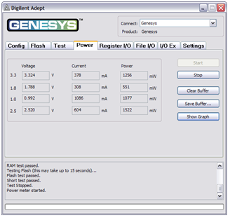
The power application provides highly-accurate (better than 1%) real-time voltage, current, and power readings from four on-board TI power-supply monitors. The monitors are based on the TI INA219 high-side current and power monitors, which are configured to return 16-bit samples for each channel at 16Hz, with each returned sample being the average of 128 sub-samples. A 5mOhm shunt resistor and selected INA219 gain setting provide 4mV and 2mA measurement resolution.
Real-time voltage, current, and power data is displayed in tabular form and updated continuously when the power meter is active (or started).
Historical data is available using the Show Graph feature, which shows a graph with voltage, current, and power plots for all four power supplies for up to ten minutes. Recorded values are also stored in a buffer that can be saved to a file for later analysis. Save Buffer and Clear Buffer are used to save and clear the historical data in the buffer.
Register I/O
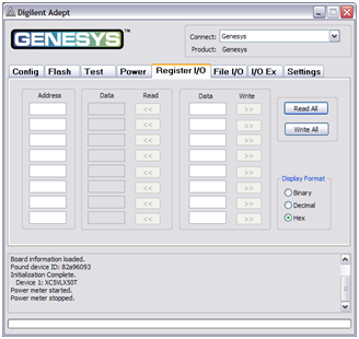
The register I/O tab requires that a corresponding IP block, available in the Parallel Interface reference design (DpimRef.vhd) on the Adept page of the Digilent website, is included and active in the FPGA. This IP block provides an EPP-style interface, where an 8-bit address selects a register, and data read and write buttons transfer data to and from the selected address. Addresses entered into the address field must match the physical address included in the FPGA IP block.
Register I/O provides an easy way to move small amounts of data into and out of specific registers in a given design. This feature greatly simplifies passing control parameters into a design, or reading low-frequency status information out of a design.
File I/O
The File I/O tab can transfer arbitrarily large files between the PC and the Genesys FPGA. A number of bytes (specified by the Length value) can be streamed into a specified register address from a file or out of a specified register address into a file. During upload and download, the file start location can be specified in terms of bytes.
As with the Register I/O tab, File I/O also requires specific IP to be available in the FPGA. This IP can include a memory controller for writing files into the on-board DDR2 and Flash memories.
I/O Expand
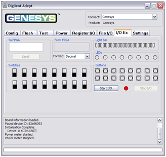
The I/O Expand tab works with an IP block in the FPGA to provide additional simple I/O beyond the physical devices found on the Genesys board. Virtual I/O devices include a 24-LED light bar, 16 slide switches, 16 push buttons, 8 discrete LEDs, a 32-bit register that can be sent to the FPGA, and a 32-bit register that can be read from the FPGA. The IP block, available in the Adept I/O Expansion reference design (AdeptIOExpansion.zip) on the Adept page of the Digilent website, provides a simple interface with well-defined signals. This IP block can easily be included in, and accessed from, user-defined circuits.
For more information, please see the Adept documentation available at the Digilent website.
Power Supplies
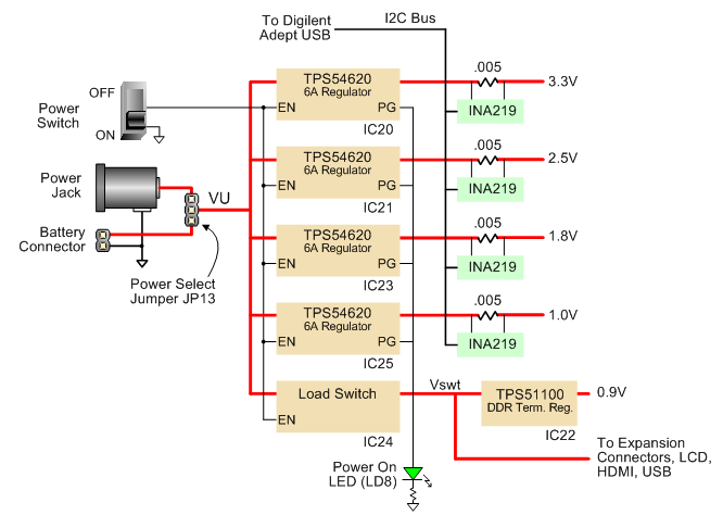
The Genesys board requires an external 5V 4A or greater power source with a coax center-positive 2.1mm internal-diameter plug (a suitable supply is provided as a part of the Genesys kit). Voltage regulator circuits from Texas Instruments create the required 3.3V, 2.5V, 1.8V, 1.0V, and 0.9V supplies from the main 5V supply. The table below provides additional information (typical currents depend strongly on FGPA configuration; the values provided are typical of medium size/speed designs).
| Table 1: Genesys Power Supplies | |||
| Supply | Circuits | Device | Amps (max/typ) |
| 3.3V | FPGA I/O, Video, RS-232, USB, Clocks, ROM, Audio | IC20: TPS54620 | 6A / 700mA |
| 2.5V | FPGA Aux, VHDC, Ethernet PHY I/O, GPIO | IC21: TPS54620 | 6A / 400mA |
| 1.0V | FPGA Core, Ethernet PHY core | IC25: TPS54620 | 6A / 0.8 – 1.2A |
| 1.8V | DDR & FPGA DDR I/O | IC23: TPS54620 | 6A / 1A |
| 0.9V | DDR SODIMM Termination Voltage (VTT) | IC22: TPS51100 | 3A / 1A |
The four main voltage rails on the Genesys board use TI INA219 power supply monitors to continuously measure voltage, current, and power. Measured values may be viewed on a PC using Digilent’s power meter that is a part of the Adept software.
Genesys power supplies are controlled by a logic-level switch (SW9) that enables/disables the power supply controller IC’s. A power-good LED (LD8), driven by the “power good” outputs on all supplies, indicates that all supplies are operating within 10% of nominal.
A load switch (the TPS51100) passes the input voltage VU to the “Vswt” node, depending on the state of the power switch. Vswt is assumed to be 5V, and is used by many systems on the board including the LCD, HDMI ports, I2C bus, and USB host. Vswt is also available at expansion connectors, so that any connected boards can be turned off along with the Genesys board.
DDR2 Memory
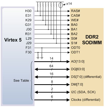
A single small outline dual in-line memory module (SODIMM) connector is provided and loaded with a Micron MT4HTF3264HY-667D3 (or equivalent) single-rank unregistered 256Mbyte DDR2 module (additional address lines and chip selects are routed, so that similar SODIMMs with densities up to 2GB may be used). Serial Presence Detect (SPD) using an IIC interface to the DDR DIMM is also supported.
The Genesys board has been tested for DDR2 operation at a 400MHz data rate. Faster data rates might be possible but are not tested.
The DDR2 interface follows the pinout and routing guidelines specified in the Xilinx Memory Interface Generator (MIG) User Guide. The interface supports SSTL18 signaling, and all address, data, clocks, and control signals are delay-matched and impedance-controlled. Address and control signals are terminated through 47-ohm resistors to a 0.9V VTT, and data signals use the On-Die-Termination (ODT) feature of the SODIMM. Two well-matched DDR2 clock signal pairs are provided to the SODIMM that can be driven with low-skew clocks from the FPGA.
| DDR2 SODIMM Pinout | |||||||||||||||
| Data | Address | Strobes | Clk,Mask,I2C | Control | |||||||||||
| DQ0: | AF30 | DQ16: | AC28 | DQ32: | V29 | DQ48: | M28 | AD0: | L30 | DS0P: | AA29 | CK0P: | AK29 | RAS#: | H30 |
| DQ1: | AK31 | DQ17: | AB25 | DQ33: | Y27 | DQ49: | L28 | AD1: | M30 | DS0N: | AA30 | CK0N: | AJ29 | CAS#: | E31 |
| DQ2: | AF31 | DQ18: | AC27 | DQ34: | Y26 | DQ50: | F25 | AD2: | N29 | DS1P: | AK28 | CK1P: | E28 | WE#: | K29 |
| DQ3: | AD30 | DQ19: | AA26 | DQ35: | W24 | DQ51: | H25 | AD3: | P29 | DS1N: | AK27 | CK1N: | F28 | BA0: | G31 |
| DQ4: | AJ30 | DQ20: | AB26 | DQ36: | V28 | DQ52: | K27 | AD4: | K31 | DS2P: | AK26 | CKE0: | T28 | BA1: | J30 |
| DQ5: | AF29 | DQ21: | AA24 | DQ37: | W25 | DQ53: | K28 | AD5: | L31 | DS2N: | AJ27 | CKE1: | U30 | BA2: | R31 |
| DQ6: | AD29 | DQ22: | AB27 | DQ38: | W26 | DQ54: | H24 | AD6: | P31 | DS3P: | AB31 | DM0: | AJ31 | S0: | L29 |
| DQ7: | AE29 | DQ23: | AA25 | DQ39: | V24 | DQ55: | G26 | AD7: | P30 | DS3N: | AA31 | DM1: | AE28 | S1: | J29 |
| DQ8: | AH27 | DQ24: | AC29 | DQ40: | R24 | DQ56: | G25 | AD8: | M31 | DS4P: | Y28 | DM2: | Y24 | ODT0: | F31 |
| DQ9: | AF28 | DQ25: | AB30 | DQ41: | P25 | DQ57: | M26 | AD9: | R28 | DS4N: | Y29 | DM3: | Y31 | ODT1: | F30 |
| DQ10: | AH28 | DQ26: | W31 | DQ42: | N24 | DQ58: | J24 | AD10: | J31 | DS5P: | E26 | DM4: | V25 | ||
| DQ11: | AA28 | DQ27: | V30 | DQ43: | P26 | DQ59: | L26 | AD11: | R29 | DS5N: | E27 | DM5: | P24 | ||
| DQ12: | AG25 | DQ28: | AC30 | DQ44: | T24 | DQ60: | J27 | AD12: | T31 | DS6P: | H28 | DM6: | F26 | ||
| DQ13: | AJ26 | DQ29: | W29 | DQ45: | N25 | DQ61: | M25 | AD13: | H29 | DS6N: | G28 | DM7: | J25 | ||
| DQ14: | AG28 | DQ30: | V27 | DQ46: | P27 | DQ62: | L25 | DS7P: | G27 | SDA: | F29 | ||||
| DQ15: | AB28 | DQ31: | W27 | DQ47: | N28 | DQ63: | L24 | DS7N: | H27 | SCK: | E29 | ||||
Flash Memory
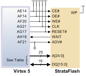
The Genesys board uses a 256Mbit Numonyx P30 parallel flash memory device (organized as 16-bit by 16Mbytes) for non-volatile storage of FPGA configuration files. Configuration files are stored using the byte-peripheral interface mode (BPI) in either up or down configurations. A single FPGA configuration file requires less than 16Mbits, leaving 140Mbits available for user data. Data can be transferred to/from the Flash by user applications, or by facilities built into the Adept software. A reference design on the Digilent website provides an example of driving the Flash memory.
| Address Signals | Data Signals | ||||
| A0: | K12 | A13: | K16 | D0: | AD19 |
| A1: | K13 | A14: | K21 | D1: | AE19 |
| A2: | H23 | A15: | J22 | D2: | AE17 |
| A3: | G23 | A16: | L16 | D3: | AF16 |
| A4: | H12 | A17: | L15 | D4: | AD20 |
| A5: | J12 | A18: | L20 | D5: | AE21 |
| A6: | K22 | A19: | L21 | D6: | AE16 |
| A7: | K23 | A20: | AE23 | D7: | AF15 |
| A8: | K14 | A21: | AE22 | D8: | AH13 |
| A9: | L14 | A22: | AG12 | D9: | AH14 |
| A10: | H22 | A23: | AF13 | D10: | AH19 |
| A11: | G22 | A24: | AG23 | D11: | AH20 |
| A12: | J15 | D12: | AG13 | ||
| D13: | AH12 | ||||
| D14: | AH22 | ||||
| D15: | AG22 | ||||
A board test/demonstration program is loaded into the StrataFlash during manufacturing. That configuration, also available on the Digilent webpage, can be used to demonstrate and check all of the devices and circuits on the Genesys board.

