

Welcome to the first expanded explanation post in our series on the ‘Components of an FPGA’. This post will describe the architecture of a configurable logic block (CLB) and the functionality this component serves within a field programmable gate array (FPGA). There is not a strict standard to the architecture of a CLB in any particular FPGA, so the information in this post is specifically regarding CLBs found in Xilinx 7 series FPGAs. For a broader look, check out our article on the structure of an FPGA.
A CLB is the fundamental component of an FPGA, allowing the user to implement virtually any logical functionality within the chip. This is achieved by the usage of two sets of similar components within a block, known as slices. There are two different types of slices, referred to as SLICEM and SLICEL, and each CLB can contain either a SLICEM and SLICEL or two SLICELs. There are roughly twice as many SLICELs than SLICEMs on a chip, though the exact numbers vary by device. These slices contain four look-up-tables (LUTs), eight flip-flops (FF), a network of carry logic, and three types of multiplexers. In an effort to avoid getting lost before we really begin, here is a crude diagram illustrating this internal structure.

And to itemize: one CLB = 2 slices, one slice = 4 LUTs + 8 FF. Therefore, one CLB = 8 LUTs + 16FF. This numerical summary is just to provide an accurate picture of what the contents of a CLB specifically are. Now let’s get into a more detailed description of each piece.
SLICEM and SLICEL
The components discussed after this all exist as pieces within a slice. This fact does not mean that the whole is simply the sum of its parts! There are some unique features to the slices themselves that allow an FPGA to expand its functionality.
First, the slices within a CLB are not connected to each other. They are physically oriented in a similar fashion to the above diagram so that they may be connected with the same slice type (SLICEM or SLICEL) within CLBs above or below, creating columns. This allows interconnections between SLICEM or SLICEL in a column to create large scale functions.
The distinguishing feature of the two slice types is the configurability of the SLICEM. SLICEM can be configured so that the look-up tables within it can act as shift registers or as data storage (creating distributed memory on the chip) in addition to its normal logic functionality.
A note on naming: the ‘M’ may be an indication of its ability to act as distributed memory, while the ‘L’ may be an indication of its exclusive logic functionality. This is just speculative but it can be helpful to remember which is which.
Look-Up Table
Look-up tables, the cheat sheet of computing….okay, this statement may be a bit strong. It does, however, illustrate the point that a LUT can serve to speed up processing by providing a set output for a given input, rather than requiring computation on the input data.
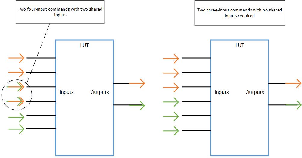
The LUTs in an FPGA (Xilinx 7 series) are designed with six inputs and two outputs. Each of these inputs and outputs are independent and allow for the LUT to be implemented in a number of ways, such as a single six-input function or two functions of five or fewer inputs, though five and four input functions will need to have a common input, while three and two input functions do not.
Confusing? Yes. Illustration? Yes!
Flip-Flops/Latches
A flip-flop is a primitive storage device that can store a single bit of information. Each slice contains eight of these storage elements. Four are available exclusively as flip-flops (synchronous storage) and the other four can be configured either as standard flip-flop or as a latch (asynchronous storage). One final caveat is that when the four that can be configured as a latch are, the other four flip-flops in the slice become unusable.
Multiplexers (Muxes)
Multiplexing within a single slice is handled in an interesting way. Instead of a large number of dedicated Muxes with fixed inputs, the flexible functionality of the LUT is used. Each LUT can be implemented as a 4:1 Mux, using two of the six inputs as selects for the other four. Larger multiplexing functionality is developed from this starting point. Two LUTs configured in this way are combined into a dedicated multiplexer (called F7AMUX or F7BMUX if the naming is significant to you) which allows you to have an 8:1 MUX. All four LUTs, through the two 8:1 Muxes, can be combined into a second type of dedicated multiplexer (F8MUX) to provide a 16:1 Mux functionality in the slice.
Carry Logic
Carry lookahead logic is implemented in each slice on a CLB with a combination of dedicated multiplexer and XOR gates that are used within the carry chain. The carry chain logic in an individual slice is four bits high and is the circuit that directly connects a column of slices together. It is possible to cascade a carry chain across multiple slices in order to quickly implement addition, subtraction, and multiplication operations on operands that are too large to be processed by a single slice (like if you wanted to add/subtract/multiply two numbers bigger than 15 or 1111 for binary speakers).
If you made it to the end here, thank you for reading! More details about the distributed memory functionality of the LUTs will be covered in the ‘Memory Resources’ follow up along with on-chip block RAM. Details on the background for the logic components and concepts presented can be found at the links below.
- Multiplexers
- Flip-Flops
- Carry Logic – this can be a bit complex, so here is the Digilent module as well as a Wikipedia article
This content is relevant to the Genesys ZU, Basys 3, Nexys A7, Cmod A7, Arty S7, Arty Z7, Cora Z7, Arty A7, Nexys Video, Eclypse Z7, Zybo Z7, and Cmod S7. All can be found on our FPGA product page.
Fine post, but for the real meat and potatoes official Xilinx documentation does a fair job. I’d recommend UG474 “Configurable Logic Block (CLB) User Guide” at https://www.xilinx.com/support/documentation/user_guides/ug474_7Series_CLB.pdf
To be frank it is not at all clear.It seems like a confusion is confusing me.