

The Basics of FPGA
A field-programmable gate array (FPGA) is an integrated circuit designed to be configured by a customer or a designer after manufacturing – hence the term field-programmable.
The FPGA can be configured many thousands of times into a virtually unlimited number of circuits, making it an ideal tool for learning about digital circuits and systems. In fact, FPGA’s have gained wide acceptance in the electronics industry for the same reason—they can quickly be configured into virtually any circuit (and even entire computer systems), allowing engineers to thoroughly study designs before they are built commercially.
Here at Digilent we frequently talk about the different applications and uses for Field Programmable Gate Arrays (FPGAs), but admittedly we rarely cover another topic… what exactly is an FPGA board, and what is FPGA used for? In an attempt to address these questions, today we will provide a brief overview of just that.
An Introduction to FPGA
Developed in the mid-1980s, FPGAs were originally conceived to give designers the ability to create custom digital logic. By the early 1990s, FPGAs were primarily used in telecommunications and networking. By the end of the 90’s, FPGAs were being used in consumer, automotive, and industrial applications, opening the way for a variety of job opportunities.
How Does an FPGA Work?
So how does FPGA work? An FPGA consists of internal hardware blocks with user-programmable interconnects to customize operation for a specific application. These interconnects can be reprogrammed, allowing the FPGA to accommodate changes to the design or support a new application during the lifetime of the part. The FPGA is programmed during the manufacturing process but can later be re-programmed to reflect any changes made to the device.
An FPGA is based on a matrix of configurable logic blocks (CLBs) connected via programmable interconnects. CLBs constitute the basic FPGA cell and includes two 16-bit function generators, one 8-bit function generator, two registers (flip-flops or latches), and reprogrammable routing controls (multiplexers). CLBs are used to implement macros and other designed functions.
Unlike processors, FPGAs are capable of parallel operations, so different processing operations do not compete for the same resources. Each independent task is assigned to a dedicated section of the chip and can function autonomously without influence from other logic blocks. Consequently, the performance of one part of the application is unaffected as more operations are added.
The FPGAs internal configuration is set by software or as it is typically referred to, “firmware.” FPGAs can be reprogrammed in the field as application or functionality requirements change.
FPGAs are designed to be programmed using Hardware Description Language such as Verilog HDL or VHDL. Because they are reprogrammable, FPGAs differ from ASIC ICs, which are designed to do specifically designed tasks.
Making a decision on if an FPGA-based design should be used needs to be made early in the design process. Considerations should be made regarding whether or not the chip will need to be re-programmed later in the design process or even after manufacturing. Sometimes manufacturers may decide on an FPGA-based design for early in the development cycle when bugs may still be found, and then switch to an ASIC when the design is stable.
What’s Inside an FPGA?
FPGAs contain components specialized for specific functions and more general-purpose configurable logic.
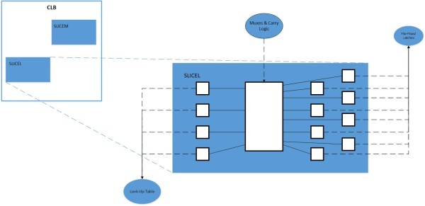
Configurable Logic Block
Configurable logic blocks (CLBs) are the basic logic unit of an FPGA. A CLB gives the FPGA its ability to accept different hardware configurations. CLBs can be programmed to perform almost any logic function. The individual CLB contains a number of discrete logic components including look-up tables (LUTs) and flip-flops.
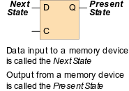
Flip-Flops
A flip-flop is a circuit that has two stable states and can be used to store state information. Flip-flops are binary shift registers that synchronize logic and save logical states between clock cycles within an FPGA circuit. A flip-flop stores a single bit of data.
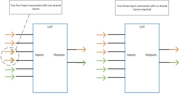
Lookup Tables
A lookup table (LUT) determines what the output is for any given input(s). In the context of combinational logic, it is the truth table and defines how combinatorial logic behaves. A truth table is a predefined list of outputs for each combination of inputs. The LUT holds a custom truth table that is loaded when the chip is powered up.
DSP Slices
A DSP slice, or sometimes referred to as a block or cell, is one of the specialized components in an FPGA. It carries out digital signal processing functions, like filtering or multiplying, more efficiently than using many CLBs. This multiplier circuitry saves on LUT and flip-flop usage in math and signal processing applications.
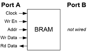
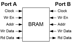
Block RAM
The memory available on an FPGA chip is referred to as block RAM or BRAM. These blocks can be subdivided or cascaded to make smaller or larger sizes of BRAM available. Digital signal processing algorithms frequently need to keep track of an entire block of data and without onboard memory. Many processing functions do not fit within the configurable logic of an FPGA chip.
Transceivers
Transceivers are made to transmit and receive serial data to and from the FPGA at high rates. This dedicated component allows for implementation of high-speed data transfer without consuming logic resources of the FPGA.
Input/Output Blocks
Input Output (IO) blocks are the components through which data transfers in and out of the FPGA. The IO blocks are configurable in several ways depending on the type of data. They operate at lower speeds than transceivers but maintain more functional flexibility.
What Are FPGA Features?
Infinitely configurable FPGA fabric allows programmers to design an FPGA to perform almost any function. In addition to the flexibility provided by FPGA fabric, FPGA throughput is extremely high because of the parallel nature of an FPGA’s design. The core capabilities of an FPGA are as follows:
Parallel processing
Parallel processing on a FPGA is possible because it does not follow the processor programming model. Parallel processing also means that slower clocks can be used (compared to high frequency clocks on processors) and users can still achieve the required throughputs, but with less energy consumption. Parallel processing also enables off-loading computer intensive parts of the application to the FPGA and relieving the processor to perform less computer intensive tasks. Parallel processing makes FPGAs excellent for working with measurement systems and edge computing applications that require processing of large amounts of data.
FPGAs can be reconfigured
More FPGA benefits! When a design needs an update or feature addition, it can be easily done. This is difficult with an ASIC. As a product evolves, feature changes or improvements can be easily made in the field by simply updating the FPGA.
Low and medium volume production
FPGAs are typically used for devices with low to medium volume. In high volume products, ASICs are typically preferred due to their lower cost. ASICs are typically cheaper for high volume products and not so cost effective for low or medium volumes. However, the initial development costs of an ASIC can be quite high, sometimes in the millions of dollars.
Rapid development process
FPGAs can offer a quick turn-around time from concept to production because no actual design at the transistor level is needed.
FPGA Uses and Applications
So what is an FPGA used for? FPGAs are used for all kinds of applications. Specific applications using an FPGA include digital signal processing, biomedical instrumentation, device controllers, software-defined radio, random logic, medical imaging, computer hardware emulation, voice recognition, cryptography, filtering and communication encoding, and more. Consumer electronics applications include smartphones, autonomous vehicles, cameras, displays, video and image processing, and security systems. Many commercial applications also make use of the FPGA advantages, like in servers, and various markets, including aerospace and defense, medical electronics, and distributed monetary systems.
What Are the Advantages of FPGA?
There are many benefits of FPGAs for embedded system design. Some advantages of FPGA are the reconfigurability, the ability to work in parallel, time-critical processing, and optimal performance, making them well-suited for numerous applications.
Performance
The parallel nature of FPGAs allows them to offer higher processing power, speeds, better response times, and overall improved performance when compared to other modern microprocessors.
Reprogrammable hardware structure
Because of the reprogrammable structure of FPGAs, functionality can be redefined even after manufacturing. Users can program new product features and functions, adapt to new standards, and reconfigure hardware applications after the product has been installed in the field. This flexibility gives FPGA-based designs advantages over microcontroller-based systems. A user can make a mistake in programming, then later modify or change the FPGA with a new configuration file and without having to create prototypes or additional hardware, saving time and reducing cost.
Quicker time to market
FPGAs are readily available and allow users to quickly develop systems based upon this technology. ASICs require manufacturing cycles taking several months. FPGA users can ship systems as soon as a product design is working and tested.
Lower overall costs
Compared to the costs of manufacturing an ASIC, FPGAs are relatively inexpensive. The design cycle for an ASIC is long and production tooling is costly. Plus, any changes in the design will require a new chip, versus an FPGA which can be simply updated with a new program.
Low maintenance
Unlike ASICs, FPGAs are reprogrammable and can be upgraded or enhanced in the field without the time and resource investment that would be required to reconfigure circuit boards and hardware. Engineering costs are also considerably lower to that of ASICs. System requirements can change over time and the cost of making incremental changes to an FPGA is small when compared to the large expense of retooling for an ASIC.
How to Learn to Design with FPGA
The first step in learning more about FPGAs is to decide on the type of chip and to choose a programing language. VHDL is more verbose than Verilog and designs written in VHDL are considered self-documenting. Verilog requires less code and is considered easier to learn. We actually talk more in depth about Xilinx’s tools in another blog post.
There are many considerations when choosing an FPGA chip, including IO count, number of gates, operating frequency, and cost. Functionality can also vary between traditional FPGAs and System on a Chip (SoC) FPGAs. SoC FPGAs integrate processor and FPGA architecture into a single device. and provide higher integration, lower power usage, smaller size, and higher bandwidth between the processor and the FPGA.
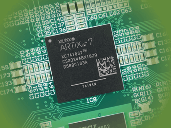
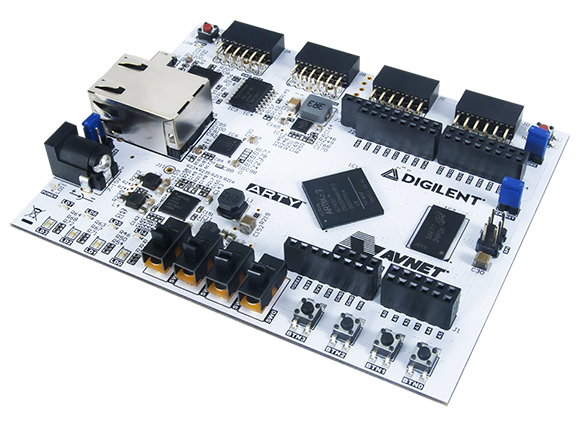
The next step is choosing a development board. The Digilent Basys 3 is ideal for getting started with FPGA. It’s an entry-level development board built around the Xilinx Artix-7 FPGA, and the Arty Z7 is a good choice for those looking to get into SoC technology. We also have a selection of other FPGA/SoC beginner boards.
Here are some additional FPGA Resources:
- The Digilent Forum is a great place to peruse previous discussions and ask fellow engineers for pointers.
- Subreddits like /r/FPGA and /r/embedded are great sources of information that changes daily.
- Nandland is a great resource with FPGA fundamentals, tutorials, examples, and videos. Here’s a great playlist to start with:
- Udemy offers an online training course on High-Level Synthesis for FPGA
FPGA is a configurable chip based on the user needs.
It run all the codes parallel.
Thank you so much for this informative post. I really like this post.