Welcome back to the Digilent blog!
So you’ve heard about FPGAs and learned that you need to download Vivado. Maybe you even found a great guide on how to install Vivado, booted it up, got the extra files that you need, went through the initial project creation in Vivado, and … now what? If this sounds more familiar than you would like to admit, then you’ve come to the right place. We’re going to walk though a series of posts over the next few days to help you get up and running with a new Vivado project including: getting any extra files you need ready to go (available here), initially setting up a Verilog project in Vivado (available here), making changes to our Verilog project and XDC file to have it work on our FPGA (the post you’re reading right now!), and finally generating the bitstream that we will use to program our FPGA. Let’s get started!
While it would be nice to think that we can simply just write up an FPGA program and configure our board with it and move on to the next program, FPGAs are complex enough that it is a good idea to add in some pre-made board files to help smooth out the programming process. I will be using Digilent’s Arty throughout the duration of this tutorial series and Verilog as my FPGA programming language of choice, as well as the 2016.4 WebPACK edition of Xilinx’s Vivado Design Suite.
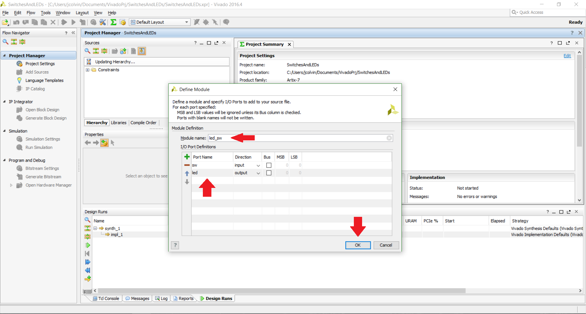
Let’s go ahead and modify our new project that we created from last time. The first window we will encounter is a wizard that lets us configure a new module; this is a part of a Verilog project where we can define the inputs and outputs for our project that we are creating. For this tutorial, we are only assigning an LED to a value of a switch, so we only need to create a single input and a single output (leaving the “Bus” box unchecked for both of them). I named my input and output “sw” and “led”, respectively, although you can name whatever you would prefer. You can also rename your module (if you kept the top.v suggestion as the file name from before, your module will currently be called “top”) to something a little more intuitive if you so desire.
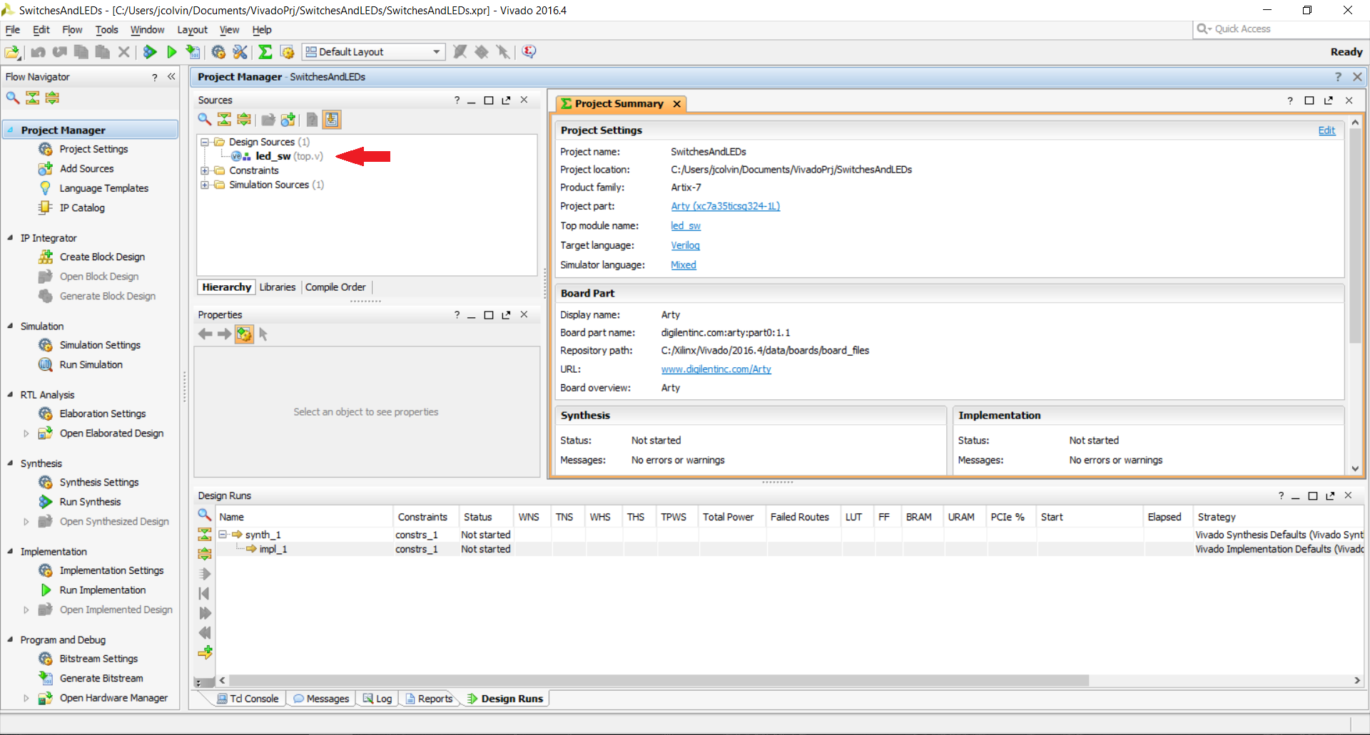
Finally, we’re at main Vivado GUI where we can actually “do stuff”, i.e. add the code to our Verilog module that tells Vivado what the module is supposed to do, change the XDC file to inform Vivado what physical pins you intend to use with your module, add IP if you choose to do so, and more. Let’s go ahead and add in the Verilog code for our top module.
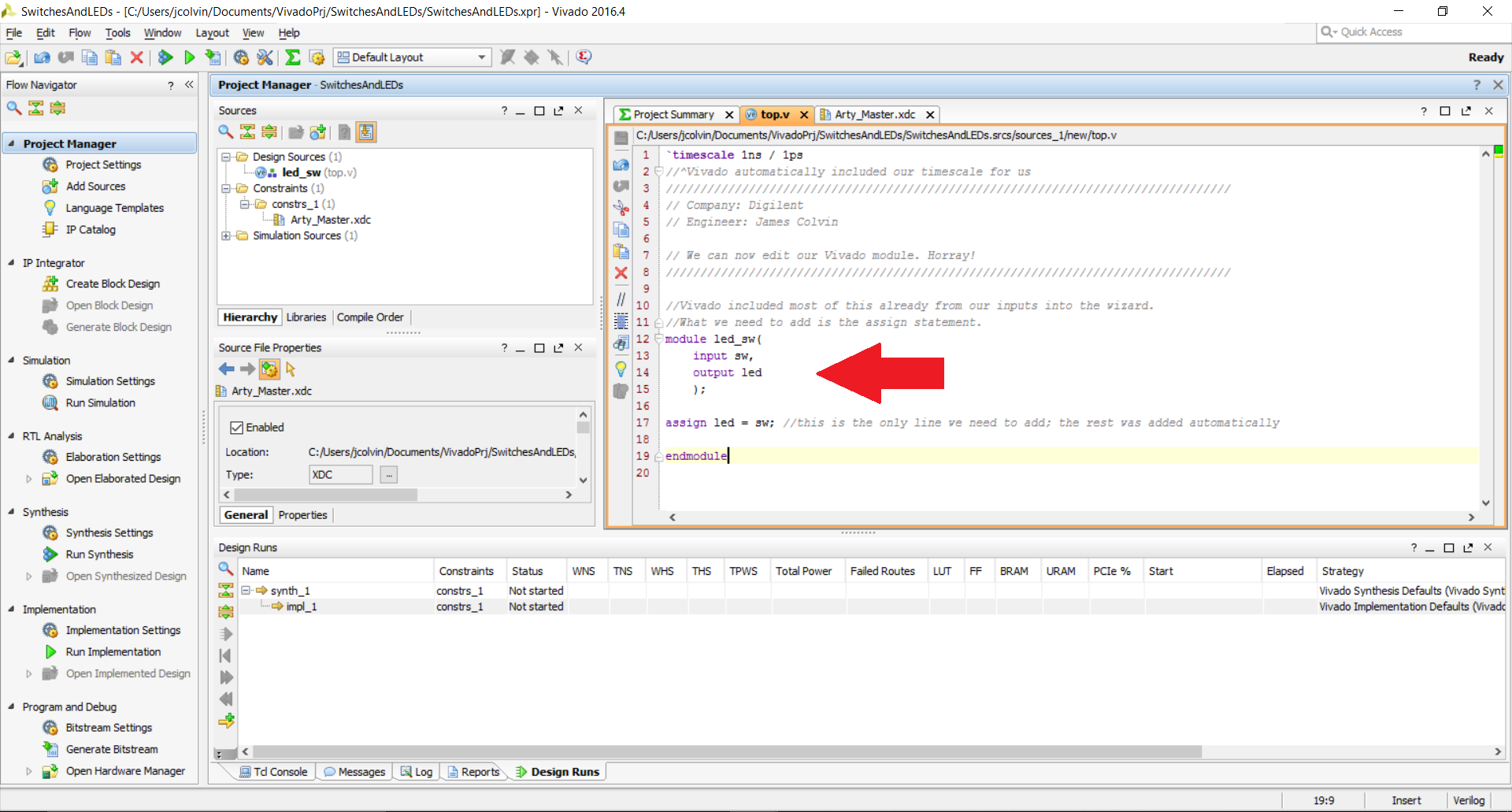
What we intend to do for this particular tutorial is have the state the LED be dependent upon the state of the associated switch. The keyword that will best model this behavior in Verilog is assign. Double click on the top module code in the Sources window in the Design Sources folder to have it open up in the editor in the upper right hand side of the GUI. The line of code that we will want to add is
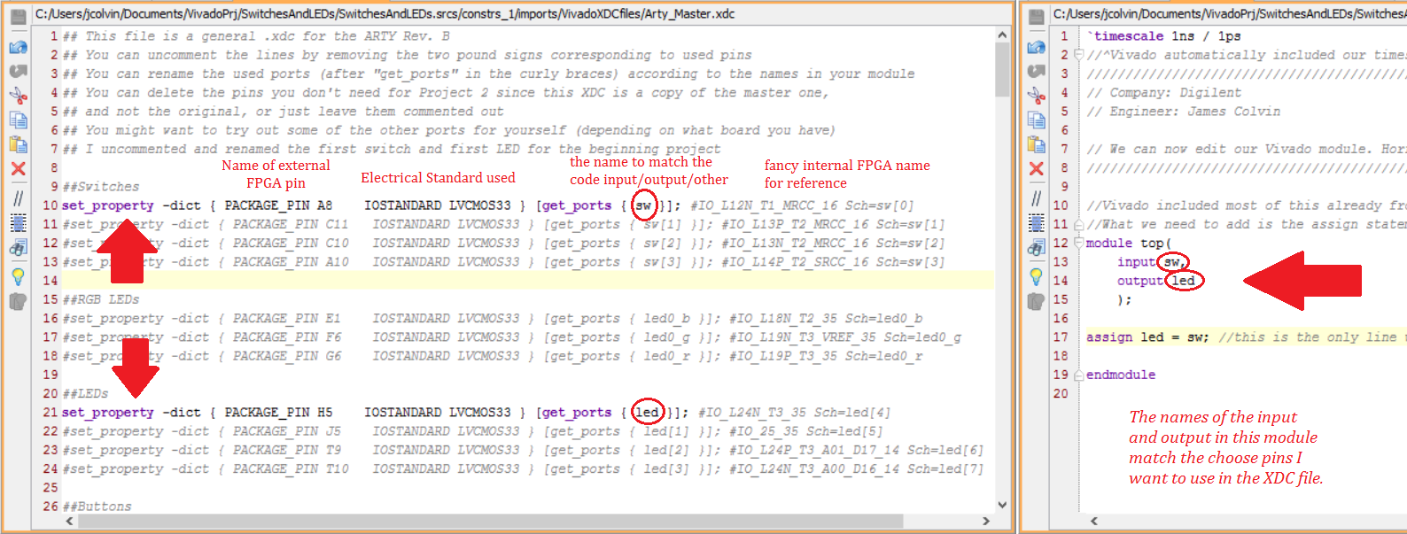
assign led = sw;It will go between the closing curly brace and semicolon surrounding our named module that we just created in the wizard. That’ll all be that we need to do in the Verilog Module for this project.
The XDC file will require a little more manipulation and is the focal point of what makes FPGAs so versatile to the end user; when this file is edited, we are in essence informing Vivado where all of our inputs and outputs on our “black box” are physically located on the FPGA. Vivado does all the heavy lifting in terms of how to actually connect point A to point B using the HDL we created in the Verilog module, while we just have to worry about some external aesthetics. Naturally, this analogy falls short once you get into more complex designs, but it’s fun to think that way. But back to the XDC file itself; how do we actually edit it?
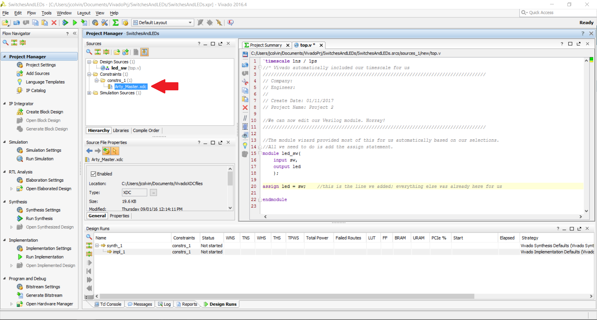
You can find the XDC file in the upper left corner in the Sources window in the Constraints folder. Double-clicking on it will bring up the XDC file in the upper riht hand side of the Vivado GUI. If you are using a master XDC file for a Digilent board, you will notice that everything in the XDC file is currently commented out with a # sign so that Vivado does not interpret it as code to be used. What we will want to do with this project (having the state of a LED be assigned to the state of a switch) is enable our LED and switch of choice.
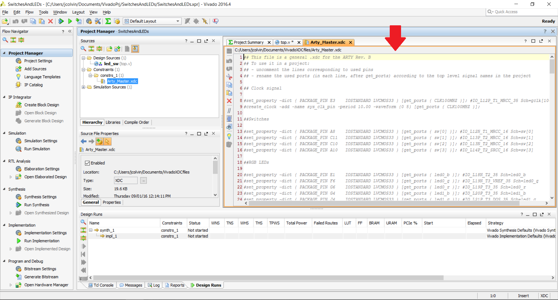
It’s important to note here that we can’t just use any pin for our LED and switch, despite how I described the XDC file in the previous paragraph. As I am looking to use one of the embedded switches and LEDs already present on the Arty (as that is my board of choice), those components are already pre-wired to a pin on the FPGA and can’t be re-routed without making physical modifications to the board. However, if I instead had an external switch and LED, in theory I could then attach those to any pin in the FPGA that I could physically access. While this might not seem all that different from a microcontroller, this really comes into play when you start to create hardware controllers but can place as many as you want wherever you need to rather than being limited to whatever that microcontroller has built into it.
The Digilent master XDC files are organized by physical group on the FPGA, such as switches, Pmod Headers, Ethernet PHY, and the like. For this tutorial project we can scroll down to the switches and LEDs section and uncomment a single line from both of them by removing the # sign from the front of the associated line of code. Then, we need to edit the name of the pin (between the curly braces immediately following the get_ports statement) to match whatever we called it in our Verilog module.
Phew! The Verilog module and XDC file are edited and ready to go! After saving this project, we’ll then be able to generate our bitstream and program the FPGA which will be the final post in this tutorial series! Additionally check out our Wiki for more resources on this project.

