

What is I2C? A question I asked myself a couple months ago that I am glad to answer now! I2C (also called IIC and typically pronounced I-squared-C) stands for Inter-IC or Inter-Integrated-Circuit, was developed by Philips Semiconductor in 1982, and is one form of electronics protocol: how electronic devices communicate data with each other. I will discuss the basics to understanding I2C protocol, then show an example of debugging I2C with the Analog Discovery 2 and the Logic Analyzer and Protocol Analyzer in WaveForms.

Get stoked. Photo from here.
The way that I2C works is what makes it a very popular choice for electronics protocol. The most immediate benefit to I2C over other protocols is that multiple master and multiple slave devices can all communicate data on the same bus with the caveat that master devices can not directly communicate with each other and must “take turns” when communicating with the slave devices. UART is restricted to communication between two devices and SPI can have multiple slave devices but at the cost of more Slave Select wires and still being restricted to a single master device. I2C is generally a 2-wire system: SDA (serial data line) and SCK (serial clock, sometimes shown as SCL), although ground and power lines may be present as well.
As cool as this is, at this point you may be wondering.. how do multiple master and multiple slave devices send data over a shared, 2-wire bus?
![]()
I2C data transfer general example. Photo from here.
The ICs used in I2C operate with open-drain (FET) or open-collector (BJT) output stages. What that means is that the output of the IC is connected internally to the gate/base of a transistor, the source/emitter is connected internally to ground, and the drain/collector is externally connected to a pull-up resistor (“open” to connection outside of the IC). Since the pull-up resistor does not need to be connected to the IC power supply (which would be 5V or lower), the output can be connected to devices operating at voltages beyond the limitations of the chip. More than one of these chip outputs can be connected to the same wire while sharing the same pull-up resistor since only one output will be active at any particular time.
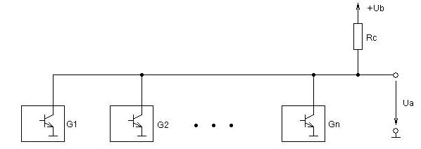
A general schematic to illustrate an open collector circuit. Photo from here.
The output transistor acts as a switch for the chip: when the IC output is applied to the gate/base of the transistor and the threshold voltage is exceeded, the transistor turns on and drives the drain/collector to nearly 0V. When no output from the IC is applied to the gate/base of the transistor, the transistor is “off” and results in an open circuit at the drain/collector which restores it to a logic level high. So, when any chip output becomes active, it drives the output to a logic level low and can only drive it low. Since no device can drive the data line high, this prevents a few undesirable circumstances: competing driving signals (one low and one high) which could cause a short from the power supply to ground, damage to chips/drivers, and excessive power consumption. Furthermore, this is what allows the data line to be bidirectional between master and slave devices.
Master and Slave, they share the road. Photo from here.
Master devices are what drives the SCK signal and initiates data transfer to/from slave devices. Each device connected to the I2C bus is software addressable by a unique address. The process of how a master device communicates with slave devices has three main parts: the Start Condition, Data Transfer, and Stop Condition. Recalling that both SDA and SCK idle at logic level high, the Start Condition is defined as when the master device pulls the SDA line to logic level low, while leaving SCK at logic level high. After one clock cycle, communication begins between master and slave devices. When the data transfer is over, the Stop Condition is initiated by the master device and is defined as leaving the SDA line pulled down and releasing the SCK line allowing the pull-up resistor to drive the SCK line to logic level high. After one clock cycle in this state, the SDA line is released and that pull-up resistor returns it to a logic level high.
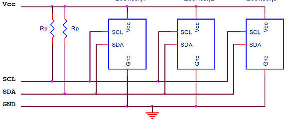
Below is an example schematic of an I2C system. Photo from here.
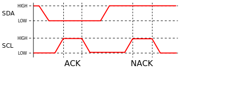
Lastly, for our introduction to I2C, the data transmission itself has a few intrinsic characteristics. Data is sent byte-wise (8 bits) with an additional Acknowledge Bit (ACK). ACK is the 9th bit in the sequence and is left low when SCK is high. This is to “acknowledge” to the transmitter that the receiver successfully read the byte of data and that another byte can be sent. If the SDA line is high on the 9th bit, then it is called a Not Acknowledge (NACK) and is basically an error message. This is the Stop Condition mentioned earlier. SDA being a single wire, the transmitter and receiver must take turns pulling it down for ACK/NACK to occur. If you wish to dive further into the nitty gritty of the different data transmission characteristics, more detailed information from the Digilent documentation resources is available here.
Below is a graphical example to distinguish between ACK and NACK. Photo from here.
Before you run off to get started on your own I2C project, I want to show you a visual example of I2C protocol in action using the Analog Discovery 2 and the Logic Analyzer (to show the individual signals) and the Protocol Analyzer (to show the overall communication) in WaveForms. I built the project found here that uses an Arduino Uno, Pmod AD2, and Pmod CLS to convert an analog input to a digital display of the input value.
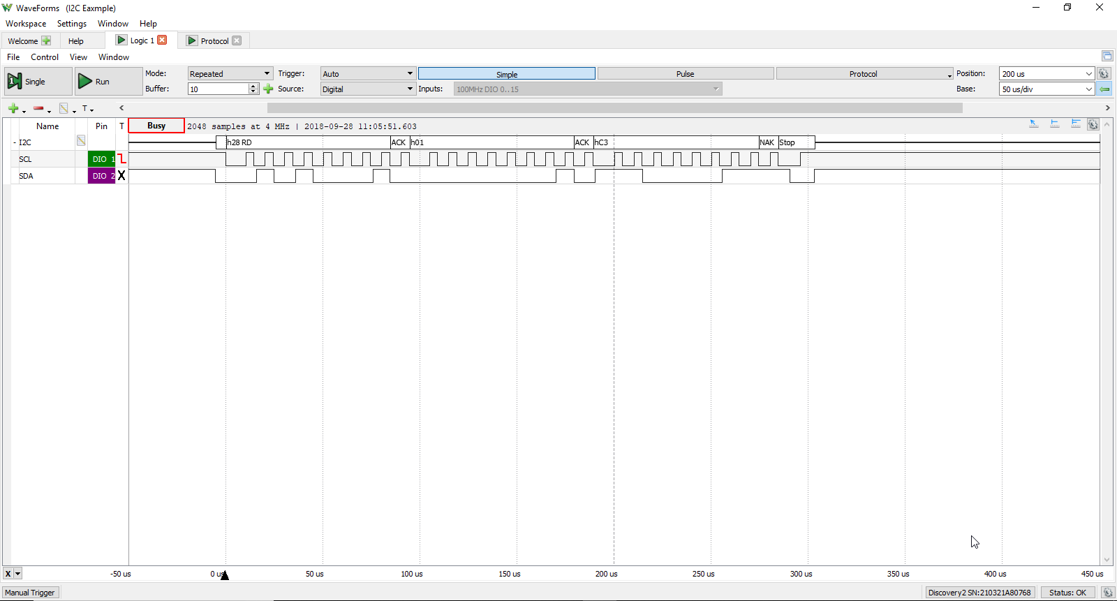
Below is a view from the Logic Analyzer. Right-click on the picture and open in a new tab to see a larger version. We can see the Start Condition happens right before time = 0 seconds. Then, 8 clock cycles gather 8 bits of data (as we are expecting) before the ACK/NACK 9th bit. We can also see that this particular system is gathering data in 3-byte chunks before initiating the Stop Condition. The data result is displayed as a hexadecimal value in the I2C logic line including the ACK/NACK result and Stop Condition.
Below is a view from the Protocol Analyzer. Right-click on the picture and open in a new tab to see a larger version. We can see the data being written to, and read from, memory, the hexadecimal result of the input analog voltage conversion (which is nearly constant in this case because I wasn’t changing the input analog voltage), the ACK/NACK bit (only NACK in this case), and the Stop Condition. This is a great way to streamline debugging without analyzing logic signals.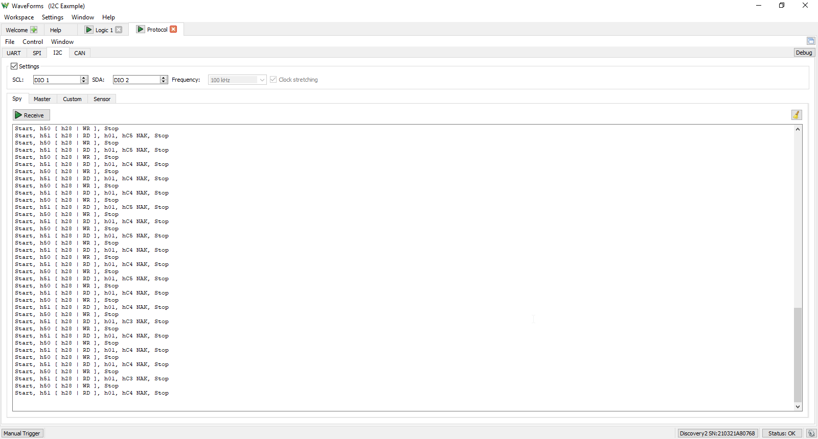
The data was from different points in time so don’t try too hard to connect the two screenshots. The Protocol Analyzer and Logic Analyzer are key tools that can help debug I2C protocol if your project doesn’t seem to be operating or communicating properly. There are more, finer details to each I2C system than discussed here so make sure you are checking out your data sheets.
Thanks for reading!
Thanks for sharing! Would I2C be considered as a half-duplex protocol?
~Natsu
Hi Natsu!
From my understanding, yes, I2C can be considered a half-duplex protocol. Half-duplex protocols are bidirectional with the channel being used interchangeably by the connected devices, which is what I2C is doing. Thanks!