

A classic interaction between a new FPGA user and an embattled older engineer (whether on our Forums or elsewhere) goes as follows:
New engineer: My design doesn’t work, could you help me figure out why?
Experienced engineer: Sure…
New engineer: Here’s a 200 line module I wrote, when I run it in hardware, it doesn’t do what I expect.
Experienced engineer: *Sighs*, Hey you should really simulate this, it’s not that hard.
New engineer: <Some kind of brain exploding emoji>
Simulation of hardware designs (which is performed using a simulator) is a way of looking at what a design does and how it responds when it receives certain signals, without running anything on an actual board. This makes it a really quick way to check your work quickly without extensive testing in hardware. It also lets you test only specific smaller parts of larger designs, letting you check that smaller pieces work, without involving the complexity of the rest of the system, and without generating an entire bitstream for a larger system – you can test a small piece in minutes instead of spending hours with debuggers and logic analyzers.
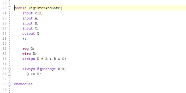
Check out the guide below to see how a design behaves as its input changes using Vivado’s build-in Simulator. The design consists of a three-input AND gate and a D-Flip-Flop to register the output.
Inventory
- This guide was written using Vivado 2022.1, however other versions will work largely the same, with some minor visual differences.
- If you haven’t already, check out Installing Vivado, Vitis, and Digilent Board Files for instructions on how to install Vivado
Guide
Simple D-Flip-Flop Example
To get started, we will add a simulation source file to our project. See Getting Started with Vivado for Hardware-Only Designs if you require a review of creating a simple design project. For the purposes of this guide, the following module is the design under test:
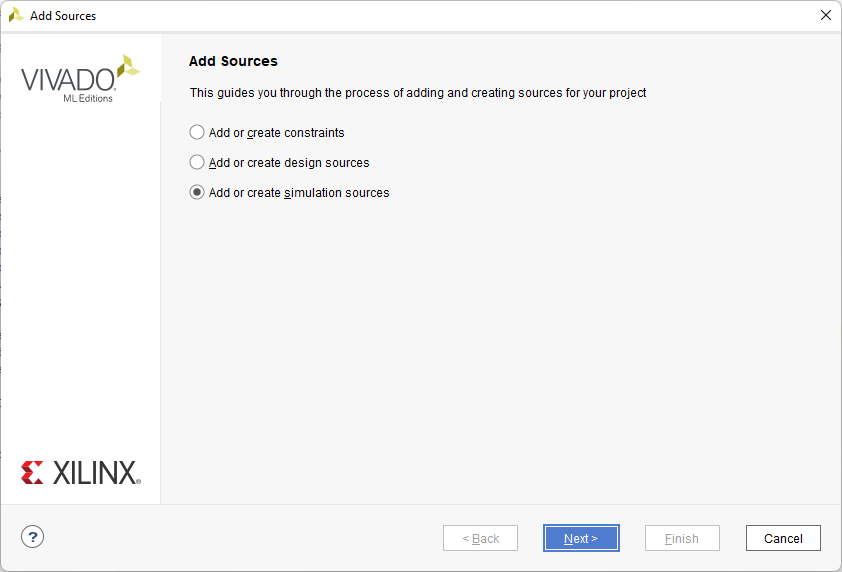
Under the Project Manager section, choose Add Sources and create a simulation source file.
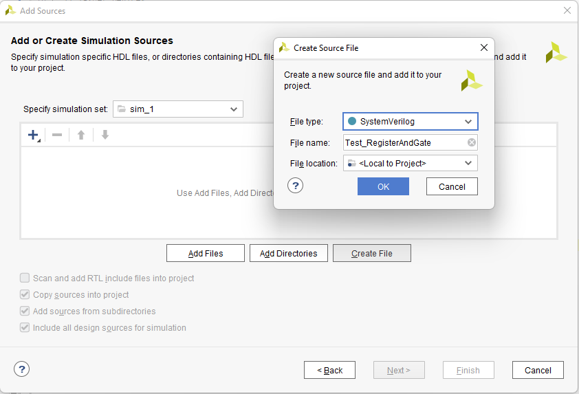
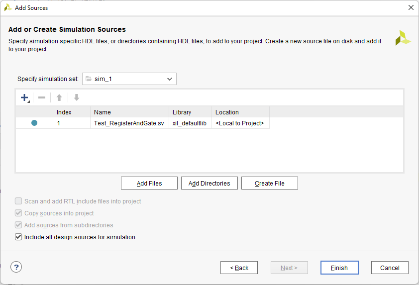
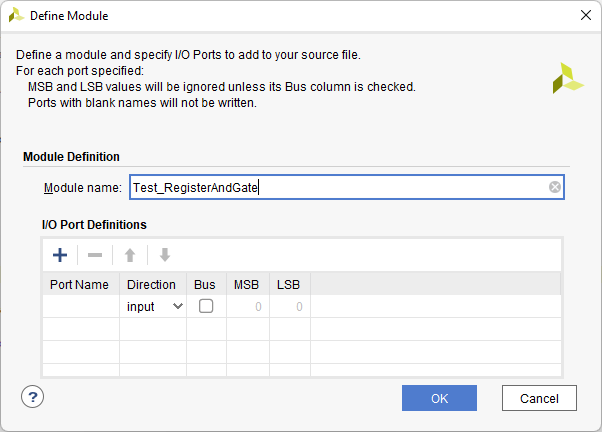
Instead of a Verilog file, we want to create a SystemVerilog file, which can be very helpful with our simulations because it exposes additional constructs. Be sure to name the file. RegisterAndGate is the name of our design module, so in order to indicate that we are running a simulation module, we will use Test_RegisterAndGate. Next, click OK and then Finish.
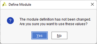
The wizard will ask if the simulation model uses inputs and outputs before you complete the process. In general, top-level test-bench modules do not use inputs or output, so press OK to continue followed by YES for confirmation.
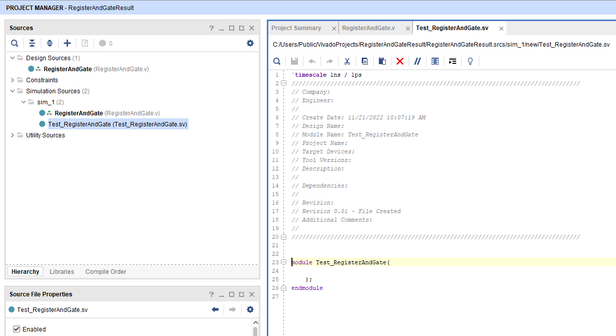
Once you double-click the new file shown under Simulation Sources→sim_1, Vivado will generate and display the file.
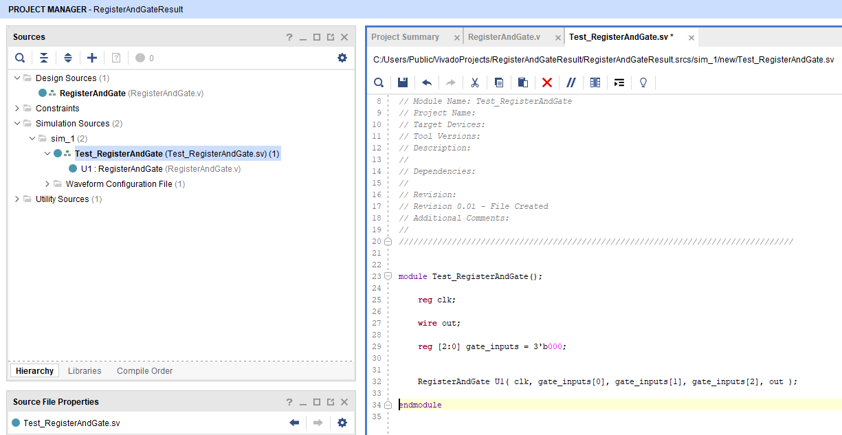
For test purposes, inputs to the module to be tested are registers and its outputs are wires. For the three inputs add one three-bit register. For the one output add a wire. Instantiate the design module as U1 (or any name of your choosing) as shown below and save the file.
Notice that under Simulation Sources→sim_1, the test module now appears as a child of the simulation module.
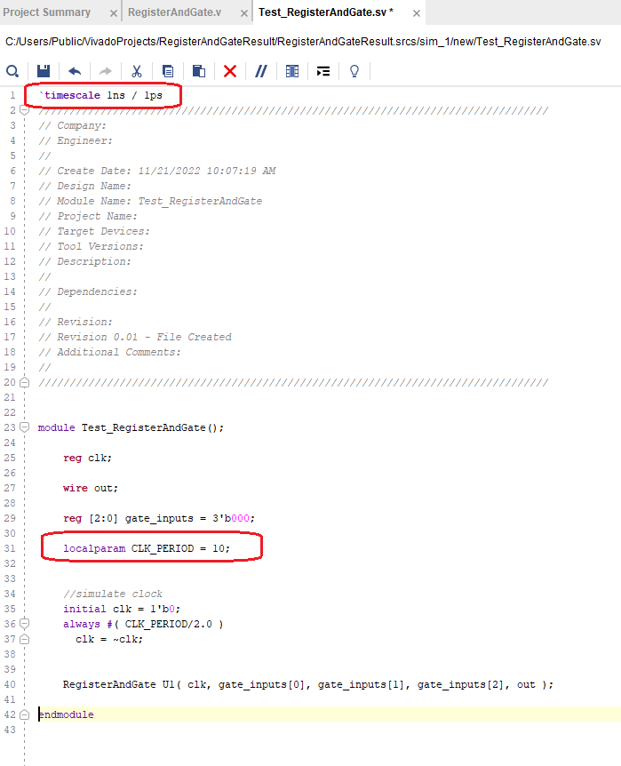
The design uses a flip-flop to register the AND gate output, so we need to create a clock next. Add a local parameter named CLK_PERIOD with a value of 10 to designate the clock period. 10 indicates 10 nS denoted by the `timescale 1ns / 1ps line at the top.
The following chunk of code initializes the clock to logic zero and toggles (inverts) it every 5 ns for as long as the simulation is running:
initial clk = 1’b0;
always #(CLK_PERIOD / 2.0)
  clk = ~clk;
Edit Test_RegisterAndGate.sv as shown to the right. This code will generate a continuous clock that has a 10 nS period. Save the file before continuing.
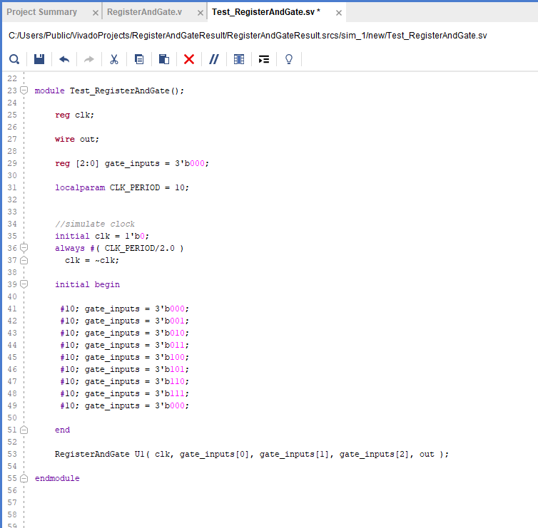
Now need the individual test steps. For this, we will use the brute-force method of individually setting each condition and time duration. See the initial-begin block below. The #10 is a 10 nS delay. Each line is a variation of the three AND gate signals along with a time delay. #10 just happens to be the period of the clock, but it is an arbitrary number. You could use #2, #3, #5, and so on, however, if the delay is shorter than the clock period, the result may not be registered to the output. Save the file and continue.
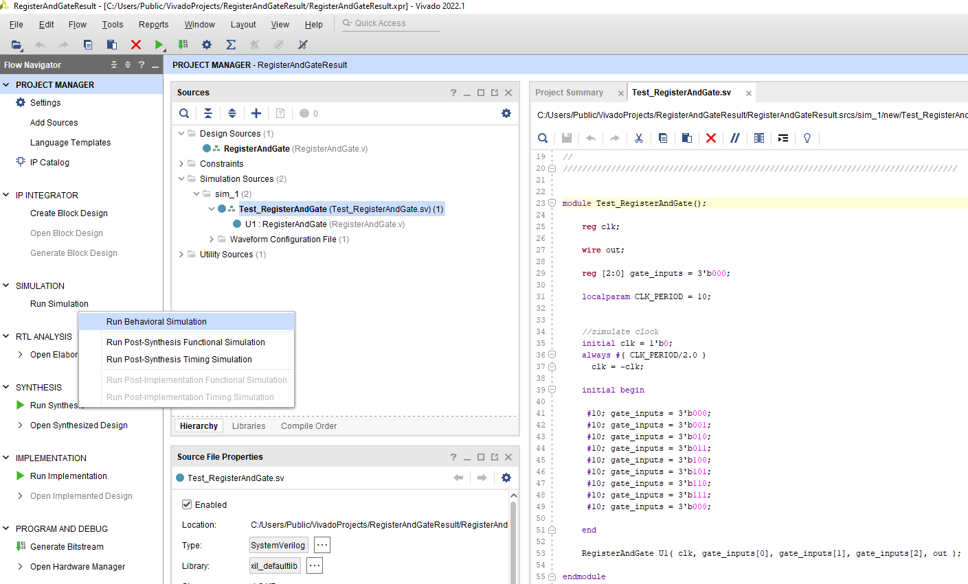
To run the simulation, choose Run Behavioral Simulation by selecting Run Simulation.
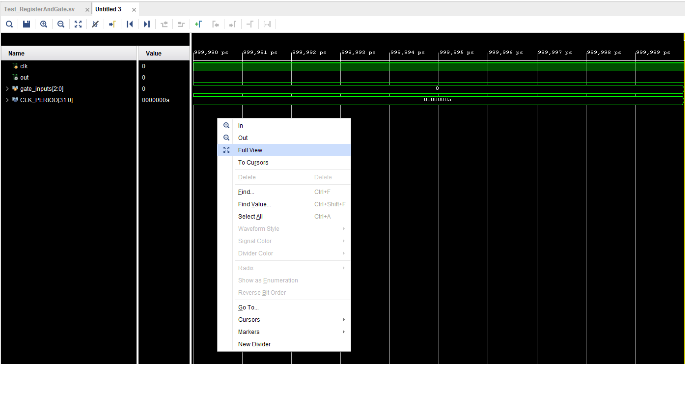
The Wave-Window should open displaying the results graphically after the simulation is done. The default period for a simulation is 1000 nS. You can adjust the time via the Simulation Settings. Select Full View and zoom in to get a better picture of the signals. To select Full View, right-mouse click the screen and choose Full View.
Hit the (+) magnifying glass icon twice then move the x-axis slider to the beginning (left) to zoom in on the main region of interest.
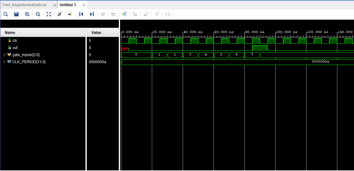
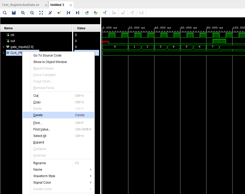
We already know what the CLK_PERIOD is, so we don’t want it cluttering up the screen. If we were taking a look at a more complex design with many more signals it would be taking up prime real estate. Go ahead and delete its trace:
To delete a signal from the Wave-Window: select it, followed by a right-click-Delete. Or select it and press the Delete key.
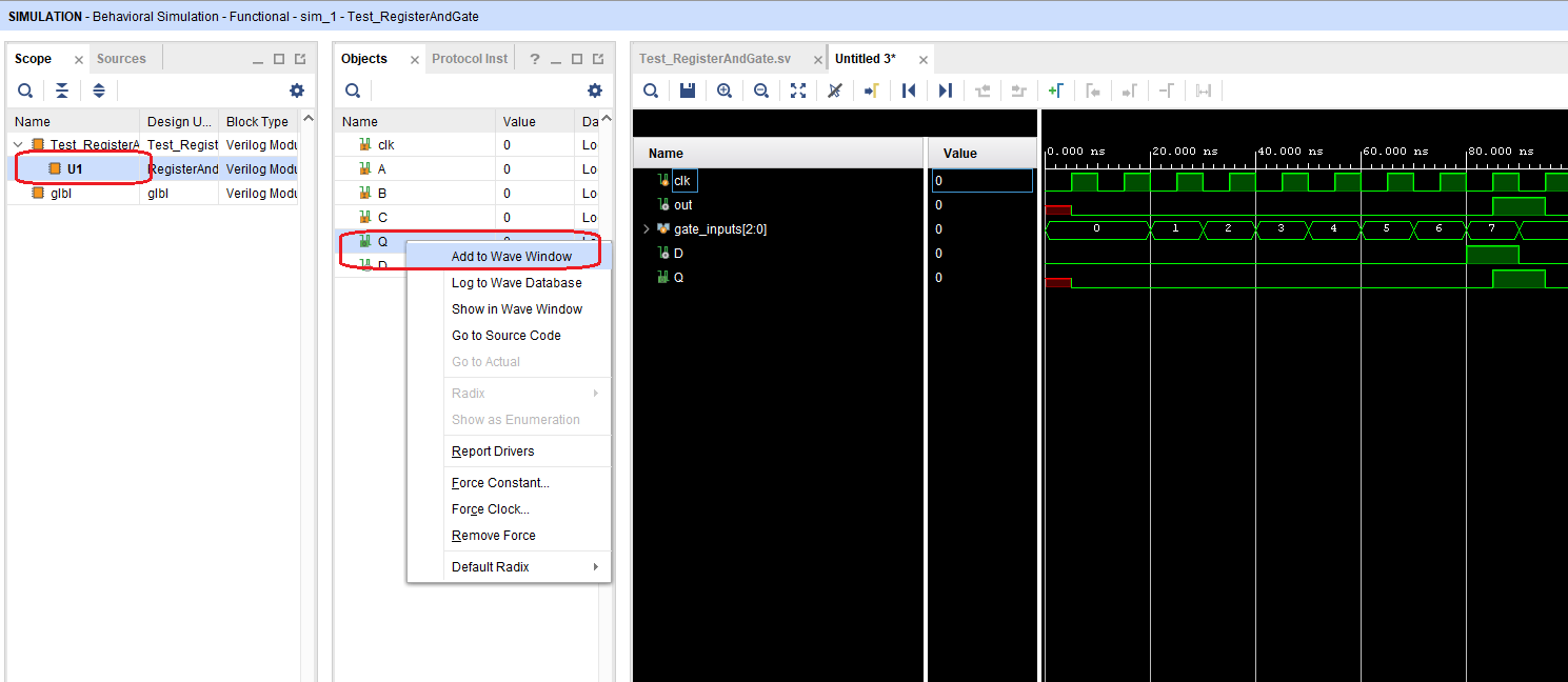
Internal signals can also be added from within the instantiated module. For instance, choose U1 (the instantiated design module) in the Scope tab. This will list the signals inside U1, right-mouse click and choose Add to Wave-Window.
These signals typically start out without recorded waves when first added to the window, so you may need to either relaunch the simulation or reset it and run it forward again in order to get these signals to appear.
From the previous Wave-window results, the gate_inputs register counts from zero to seven testing the eight combinations of the inputs. When the gate_inputs register equals seven, or all three inputs are high, the output of the AND gate is high and, on the next clock edge after, the flip-flop output Q is set high, indicating correct behavior.
In this guide on reference, you can find several additional tips and tricks, including how you can use the simulator to measure how long it takes after an event occurs for an output to appear – a useful step in verifying that your design meets the requirements you’ve been given. To jump straight to the Debouncer example, click here.
I wonder why Xilinx discontinued the testbench template generator feature in Vivado available ever since in ISE, which is simply what we use all the time to test a given FPGA simple designs. You have a “circuit.vhd”, you like to test and verify it, you simple ask for a testbench template “circuit_tb.vhd”, and then simply add stimulus and CLK processes. It is standard, available for all vendors, but now not available any more in Xilinx Vivado. This is the reason I’m using Quartus Prime + ModelSim or Questa and why I cannot use Xilinx tools any more.
regards,
This is a test bench to simulate module RegisterAndGate, but nowhere does this article show the code for that file. It would be nice to know that, so the simulation would have some relevance to the actual design being simulated.
You can find that code in the reference center! https://digilent.com/reference/programmable-logic/guides/simulation