


Editor’s Note – In this series, we will take a behind the scenes look at how an engineer tackles a project from beginning to end. What challenges will come up? How can we face problems and come up with solutions? Aside from project completion, what are successes that we can celebrate along the way?
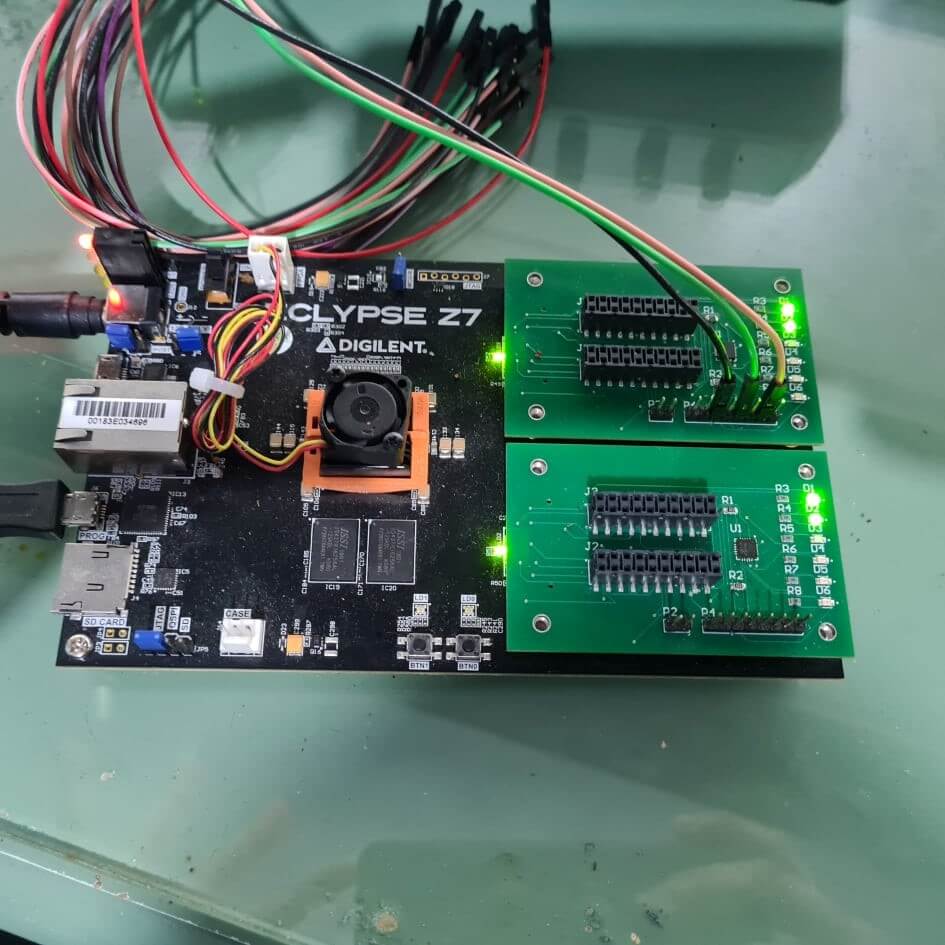
The designed PCBs (Figure 1) incorporate an attiny44a microcontroller which will act as an I2C memory. The basic function of this microcontroller is to have the SYZYGY® DNA in its flash memory and transmit this data to the platform MCU on the Eclypse Z7. Both Zmod ports on the Eclypse Z7 are compatible with version 1.1 of the SYZYGY™ specification from Opal Kelly.
The purpose of the platform microcontroller on the Eclypse is to implement SYZYGY™ SmartVIO functionality. This, among other functions, includes switching on various power supplies on the Eclypse Z7 to conform with the requirements of the Zmods connected to it. More detailed information on the SYZYGY™ standard can be found here. And more detailed information regarding the platform MCU on the Eclypse Z7 can be found here.
The designed board has been described in the previous post, however, in simple terms, the boards include the attiny44a, programming connector for MPLAB® PICkit™ 4 and output connectors which are connected to the Zmod connector, which are connected to the Zynq 7000 SoC on the Eclypse Z7.
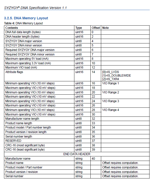
C-code for the attiny44a on the designed boards has been downloaded from SYZYGYfpga github and has been compiled and loaded into the microcontoller using Microchip Studio 7 and the aforementioned MPLAB® PICkit™ 4. The code downloaded into the microcontroller includes all the necessary functionality for the SYZYGY™ standard, but does not include the DNA data. The DNA data must be constructed and set up according to the specifications (voltages and currents) required by your new Zmod. Figure 2 below illustrates how the DNA data must be written inside the microcontroller flash memory.
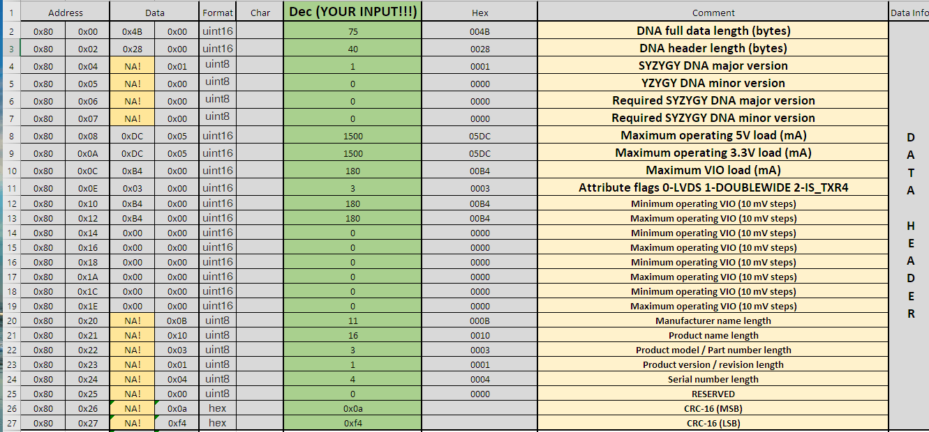
In order to set up DNA data for my RF Front End Zmod that I am designing, I have organized an Excel sheet (Figure 3). Excel is a deceptively powerful tool, especially for electronics engineers! The purpose of this Excel sheet is to convert the decimal input (green column) into hexadecimal data which will be written to the microcontrollers flash via I2C. As can be seen from Figure 3, the maximum operating current of the 5 Volts, 3.3 Volts, and VIO Voltage available on the Zmod connector have been set to 1.5 Amperes, 1.5 Amperes and 180 milliamperes. Yes, this will be quite a power hungry Zmod since it is an RF Front End which includes RF power amplification!
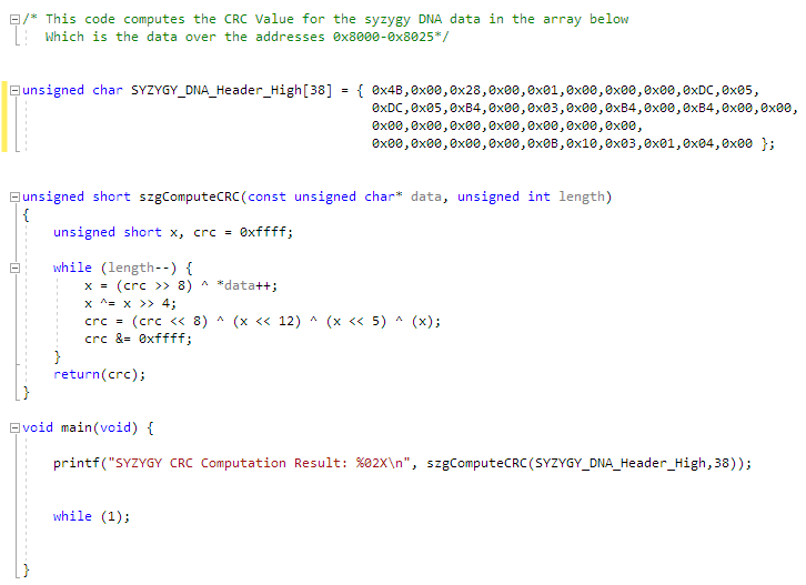
As can be seen on the bottom of the DNA data, Cyclic Redundancy Check (CRC) calculated on the DNA data header must be listed in the last two bytes of the DNA data. In order to compute the CRC according to the SYZYGY™ standard, I have organized a simple Visual Studio C program which does this for me, illustrated in Figure 4. A cell in the designed Excel sheet provides the hexadecimal DNA header data so I can simply copy and paste this into the Visual Studios program. Simply run the program and BAM! The CRC result is given. Simply insert the hexadecimal value in the Excel sheet and DNA data for your SYZYGY compliant peripheral is ready to be written on the microcontroller’s flash memory via I2C.
The DNA data will be written to the microcontroller’s flash using the Analog Discovery Pro ADP3450. In the next entry I will go over how this is done very easily and effectively using the ADP3450.
Good job.