

Constraining Ports in Block Designs
In Vivado block designs, there are a couple of different ways to manage the inputs and outputs of your design and which FPGA pin locations they are connected to. Regardless of the method used, location constraints, whether written manually or automatically generated, will always be used. Manual constraints are typed up in an XDC file (or edited from a template) using a text editor. Board-file-based constraints are created entirely within the IP integrator and generate XDC files behind the scenes. When choosing which you should use for the ports in your design, there are some tradeoffs.
Manual constraints can be easier to port from one board to another than automatic constraints. The former requires making some changes to a text file while the latter requires using automated flows to apply IP configuration settings that are required by the board. In the case of simple I/Os, like LEDs, you just need to change the pin locations in your XDC, and in most cases can continue modifying your block design without worrying about them. Also, you can switch out which LEDs are used the same way – just changing a few lines of text changes which ports things are tied to – if for example you wanted to move some of those LEDs output signals into a Pmod connector.
When using manual constraints, you aren’t locked into using a whole interface. For example, if you don’t care about the third LED on a four LED bank, you just don’t have to wire it up, potentially saving some resources (admittedly in the case of these LEDs, you aren’t saving more than a couple of logic cells). Another alternative is to include it in another interface somewhere – you could make your own UART indicator LED by tying a transmit line to a second LED output for example. On the other hand, board-file-based constraints are easier to initially set up – a couple of clicks instead of a decent chunk of time spent entering names and pin locations and cross-checking between several files – and can handle applying preset configurations for extremely complex IP for you. The Zynq PS is an example of this).
It’s recommended to mix-and-match these approaches, using some board file interfaces and some manually-constrained ports, applying using the technique that best supports your needs for a specific port.
Let’s explore some of the terms that were introduced above.
Defining Some Related Terms
So, what are the board files even doing anyway? They take a collection of pin locations (physical locations connecting the FPGA to the rest of the board) and associate them to a component, an interface, and one or more presets.
A component in this case means something like “a part on the board” – the FPGA has a component and a reset button, a DDR memory chip, or an HDMI connector would each have their own component.
An interface is a set of names for signals that connect two components – a SPI interface has a clock, chip select, and a few data lines.
An IP preset is a pre-defined configuration of an IP core, which sets it up to work for your component.
Overview of Location Constraints
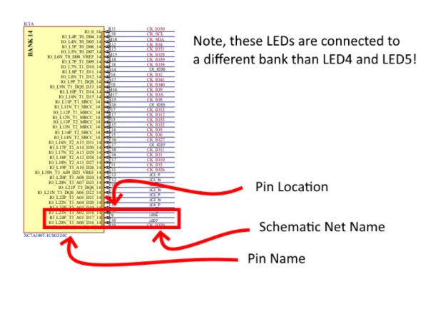
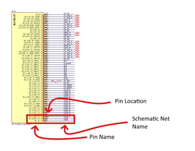
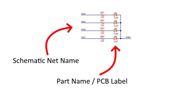
What does “constraining a port” mean? The location constraints in a Vivado project are like a map of the metaphorical edge of the FPGA chip. Physical locations on the chip, denoted by the pin names you would find in a schematic (E2, A14, VV12, or similar), are associated with the top-level ports in your hardware design, named whatever you chose to name them in the design. For a trivial example, you have an LED on your board labeled “LED4” in the schematic, physically connected to pin H5, which you want to be driven by the port “status_indicator_led” in your design. The following line of an XDC accomplishes this connection.
![]()
Importantly, the tools don’t inherently know anything about your board, and the constraint file may need to contain more information than just the location constraints. For a few examples, the logic standard of the FPGA bank that the pin is located within or the period of an input clock may be specified in an XDC. Does the FPGA bank operate on 3.3V or 1.2V or some other form of logic? How fast does all the logic being run off of this clock need to be able to run? You should always first check for vendor-provided constraint files to see what the minimum necessary constraints to use a pin are. Digilent provides these files for all our 7-series FPGA and SoC boards in the https://github.com/Digilent/digilent-xdc repository.
Board File Overview
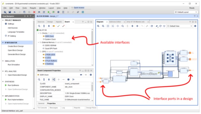
Board files, provided by FPGA board vendors (like us!) let you abstract away the details of constraint file when working within Vivado IP Integrator. These files provide additional information beyond what XDCs provide to the tools about the peripherals on the board. They do this by 1. providing all the constraints necessary for the tools to write a constraint file itself, and 2. providing preset IP configurations that you can start with to connect the entire interface a peripheral is connected to the FPGA through to a predetermined IP core capable of controlling it, thus abstracting away much of the intricacies of the physical interface. As an example, if a peripheral uses a SPI interface, the board files will typically provide the ability to add an already configured SPI controller to a design, which has the settings required to make the controller use (a) correct SPI mode for that peripheral. You typically still need to do a little bit of configuration to be able to wire up the IP to whatever you have controlling it, but this is the nature of any kind of design/integration. The constraints are entirely abstracted away, and you largely don’t need to worry about them at all (if nothing goes wrong).
When you are using an SoC board, it’s highly recommended to use the board files at least for access to the Zynq preset. This lets you use the Block Automation wizard to preconfigure the most complicated part of any Zynq design – the Zynq Processing System. This applies all the settings required to use relevant PS-connected peripherals like UART, Ethernet, SPI Flash memory controllers, and the DDR memory controller, all in only a few clicks. The same goes for using DDR with Microblaze designs.
You can find all board files for Digilent FPGA and SoC boards in the https://github.com/digilent/vivado-boards repository.
As an aside, board files are only an option when you are working with an IP Integrator design and aren’t applicable when you are writing HDL from scratch. The IP they provide configurations for are typically AXI IP, which are intended to be used with processors.
What Are Drawbacks and Workarounds of Working with Board Files?
When you work with the board files, you are generally locked into using the interfaces and IP that the creator of the board files (again, like us!) decided to include.
How do you work around this? Another way to put this would be, “What’s the hard way?”
Easy mode, with the board files: So, as an example, let’s say you have a set of LEDs you want to control from a processor, you would use the Board tab in the Vivado IP integrator to connect the LED interface to an AXI GPIO, run connection automation, and things would magically just work.
If you want to do this “the hard way”, you will add an AXI GPIO to your block design, configure it to have the correct signal direction (output only for these LEDs) and the correct bus width for your LED interface. Fairly straightforward so far. BUT, to avoid using the board files and the IP preset – which locks us into using the predefined LED interface – you need to make the AXI GPIO’s “GPIO” interface external (Make External creates an interface port for you) and constrain it – editing an imported XDC file to associate the pin locations for your LEDs with the names of the ports in your design’s LED interface.
This whole process, in both manual and automatic form, is described in excruciating step-by-step detail in this page on the wiki (which needs an intro if we link directly to it): https://reference.digilentinc.com/programmable-logic/guides/vivado-add-gpio
There’s a common snag you can run into, namely that the names of the ports in an external interface are not obvious in the IP Integrator window. So where do you find them? One quick way is to generate an HDL wrapper – this is usually one of the last steps in the process prior to generating a bitstream and fully building your project, but, critically, it gives you a place to check that what you think you designed matches what Vivado thinks you designed. If you want to know what to constrain in an XDC, this is the easiest place to check – each of the top-level ports in the design needs to be constrained to a pin location (though notably, if you are mixing both board file and manual constraints, you shouldn’t constrain the stuff your board files are handling for you).
Both board files and manual constraints are perfectly valid ways of creating your designs, but they both have their own advantages and disadvantages. Learning how each of them work is a good idea, so that you can use the technique that best suits your needs.