

Data rates on serial and parallel transmission lines are increasing rapidly. So are the data integrity issues developers face. Eye diagrams make their life easier.
Higher data rates in telecommunications and other systems that use serial or parallel data buses result in a stronger signal attenuation and larger interferences. Lines become more susceptible to noise, and clock synchronization might get problematic. Jitter, impedance mismatches, or discontinuities in cables can lead to signal distortions. All this possibly leads to data errors like missing bits or the wrong detection of zeros and ones.
Developers face the challenge of minimizing these problems. Their first step is usually to determine what effects are present in their design, and to what extent. From the information gained, they can then derive the actions necessary.
Eye diagrams are especially helpful here, as they allow a very rapid evaluation and can be used for several modulation schemes. Examples include non-return-to-zero (NRZ) systems like the Manchester code, pulse-amplitude modulation (PAM) as employed in Ethernet, DDR and USB interfaces, multi-level transmit (MLT-3) encoding, or drivers for LED lighting. For fast buses like PCI Express, USB, or for video signals, creating an eye diagram is a standard check for signal integrity.
What Is an Eye Diagram?
Now, what is an eye diagram, and what does it actually show? First of all, the “eye” is built by infinitely and persistently superimposing the individual bits (symbols) transmitted over the data line. The bit edges, rising or falling, form the vertical boundaries of the diagram, while the levels make up the horizontal limits. An ideal signal, transferred using an ideal cable, will therefore produce a rectangle with sharp edges.
But, in reality, nothing is perfect, so the eye of a real system will look very different. Already, the cable’s capacitance smoothens the slopes, and ringing creates overshoots and undershoots. Figure 1 shows an example of such a line.
Nominally, an eye diagram is nothing else than the graphical representation of the probability density function of the signal, modulo the unit interval (UI). In other words, it represents the probability with which the signal will take on a voltage during the UI. The unit interval is defined as the duration time of the symbol (nominal bit width), which is, in most instances, one clock cycle (Figure 2).
What Does an Eye Diagram Show?
When working with eye diagrams, it is important to remember that they indicate only errors belonging to the physical properties of the transmission system. They show neither logical nor protocol errors. However, as an eye diagram is a persistent display, it will also present random events. Waveforms that occur frequently are drawn with hotter colors than those that happen less often.
Generally, an eye diagram shows the extent of distortions a signal experiences as it propagates from transmitter to receiver. These distortions can have various causes and lead either to variations in the signal’s amplitudes or to edge shifts.
Impedance mismatches caused by poorly terminated cables may result in reflections, creating overshoots and undershoots of the signal and a lower voltage swing. Bad grounding schemes or crosstalk due to inferior layout of the printed circuit board (PCB) may lead to lower or higher amplitudes. The quality of cables and the make of connectors affect the signal as well. Some problems even increase with frequency, such as dielectric losses. The topology and length of a network also play a role, as do protocols, where multiple transmitters can be active at the same time during the switching phases. All these effects limit the horizontal aperture of the eye.
Edge shifts, the deviation of the signal’s edges from their expected positions and zero crossing points, are another concern, and timing jitter is one – but not the only one – cause for them. Slow rise and fall times, which result in inclining slopes of the signal’s transitions, are an issue too. Other reasons are nonlinearities of transmitters and receivers originating from their amplifiers or modulators, or from the connecting cables. Clock recovery problems also play a role. They all degrade the performance of the overall system by reducing the timing margin available for reliable signal detection. In the eye diagram, this becomes visible through the vertical obstruction of the eye.
In general, the quality of the signal amplitudes and symbol transitions can be derived from the height and width of the lines in the eye diagram. A wide-open eye means a good signal. An only slightly open or completely closed eye indicates that the receiver may no longer be able to distinguish between a 0 and a 1 signal. The open area inside the eye points to the best sampling point (decision point): the best SNR (signal-to-noise ratio) is where the eye is the widest open.
What Must Be Watched Out For?
There are a few things to keep in mind while working with an eye diagram. The placement of the oscilloscope probe is important for avoiding crosstalk and other problems. In addition, the probe’s resistance and capacitance can introduce their own errors. Moreover, the data sent should cover every bit pattern possible, so it may be necessary to create a special set of test data.
And not to forget: the measurement must run long enough to collect as much data as possible. This way, engineers can detect more distortions, as well as less frequent events.
Nevertheless, the most critical thing is the trigger. The easiest way to get the classical eye diagram is to trigger on the clock signal of the bus. If done on both slopes of the clock, all bit transitions will be captured. Although it may seem tempting to trigger on the data signal itself, this is the worst method, as longer transmissions with the same bit or bit pattern do not provide any or enough transitions for triggering. This makes it almost impossible to create a complete eye.
Other possibilities are either the divided clock trigger or the pattern trigger. The divided clock trigger is useful when the oscilloscope’s trigger input has a smaller bandwidth than the signal’s data rate. But to produce a good eye diagram, the pattern length divided by the clock’s divide ratio must not yield an integer. Otherwise, parts of the pattern will be constantly lost, while some bits will be constantly triggered on.
The pattern trigger permits displaying individual bits in the pattern by triggering on a specific sequence or pattern of data bits, allowing for a quite accurate analysis of the signal.
The last option is to trigger on a recovered clock signal, if the clock signal is embedded into the data stream, or if the relationship between clock and data got lost during the transmission. Since the recovery is computationally intensive, it is either performed by specialized hardware or downstream of the data acquisition itself. Despite its complexity, it offers some advantages, like filtering functions or adjustable parameters for the loop bandwidth, providing flexibility to optimize the eye diagram for specific measurement scenarios.
How to Create an Eye Diagram Using an ADP5250?
One oscilloscope up to these tasks is the Analog Discovery Pro ADP5250 in combination with the free WaveForms software, both from Digilent. The ADP5250 is an all-in-one, two-channel 1 GS/s 100 MHz mixed-signal oscilloscope, which is also a function generator, a power supply, and a digital multimeter (DMM). It features an analog bandwidth of 100 MHz, has 32 digital inputs and 8 I/O channels, and connects to a host computer through USB 2.0. The ADP5250 also supports frequency adjustment, a helpful feature when working with different trigger options.
WaveForms is the software for the ADP5250, and its user interface has the look and feel of traditional benchtop tools. Through it, test engineers can configure and control all the various features of the ADP5250. It has over 12 different instruments to choose from, like an oscilloscope, signal and pattern generator, data logger, spectrum, logic and network analyzers, and others. The software also includes mathematical functions, which can be used to execute numerous mathematical calculations or filters on the input channels of the oscilloscope. A software development kit (SDK) is at hand as well for further customization, as is a script editor, through which engineers can adapt the software to their needs.
How to Display an Eye in WaveForms?
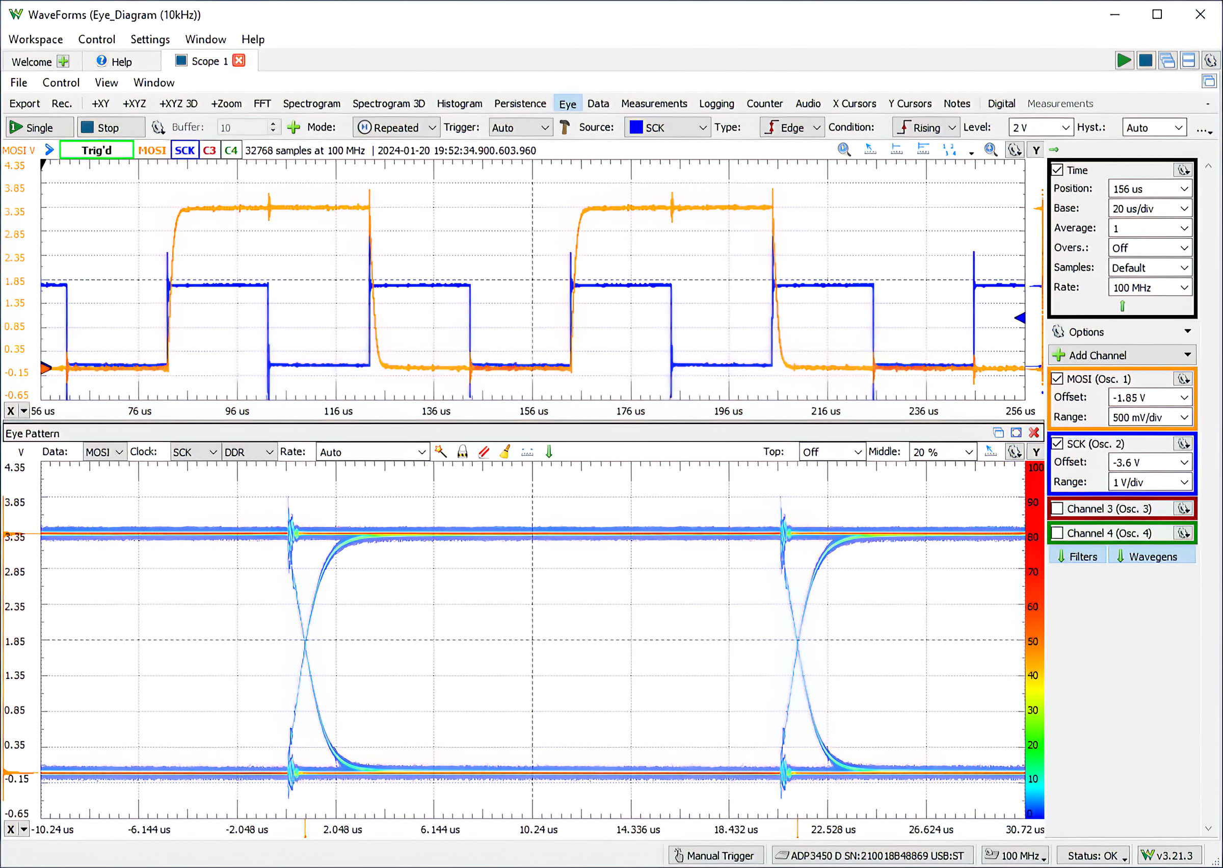
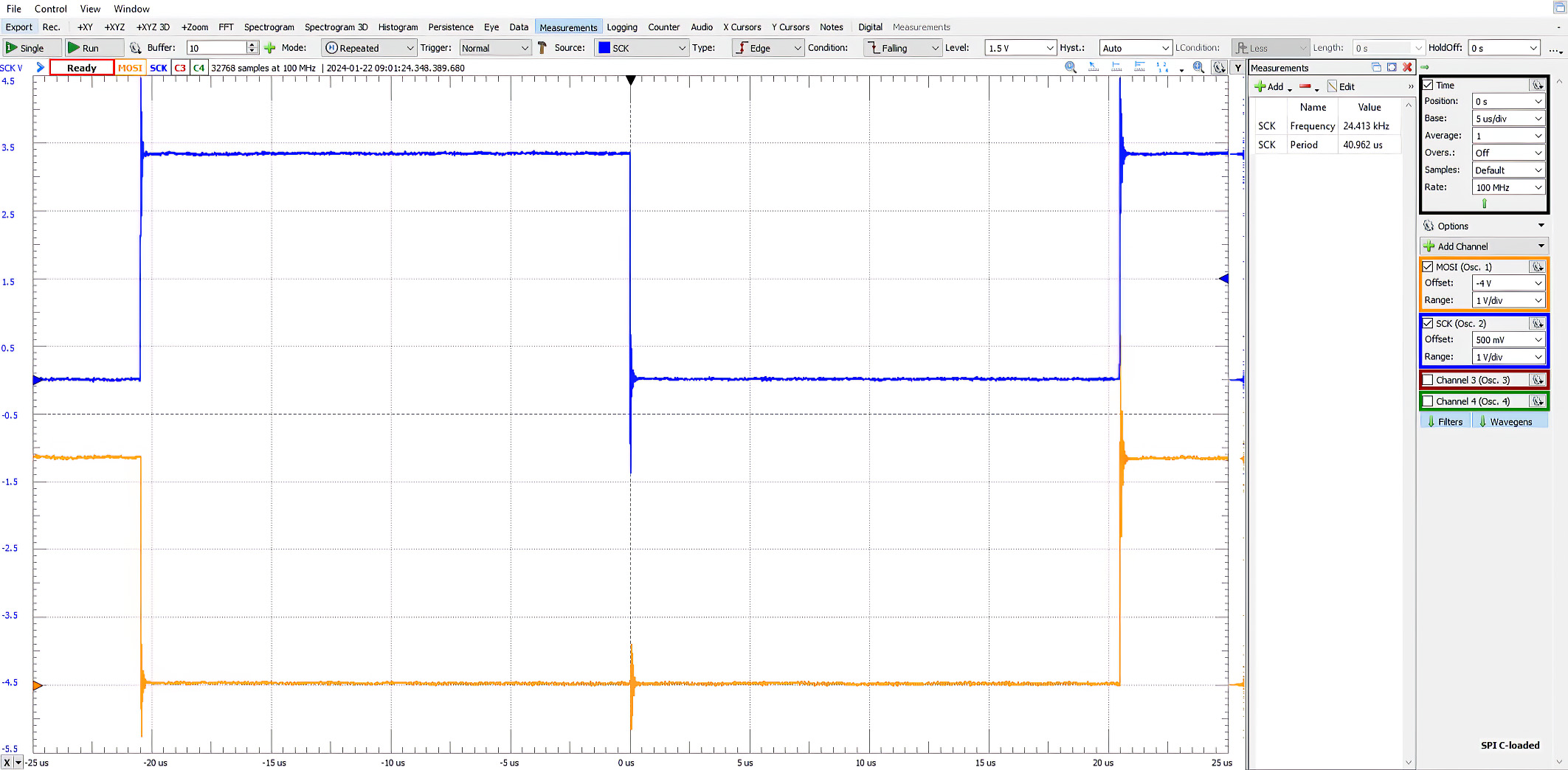
WaveForms can create eye diagrams from within the oscilloscope instrument by selecting “Eye” from the list of available views. There are only a few settings to make, and the following steps outline how the display of a simple SPI transmission can be set-up quickly. In this example, the data line (master-out slave-in / MOSI) is connected to the channel 1 of the oscilloscope, while the clock signal (SCK) is connected to channel 2. First, adjust the parameters of both channels so that they can be seen easily, and the setup of the trigger. Use SCK as the source, and “rising edge” as condition – but this depends on the actual characteristics of the SPI.
Next, display the “Eye” view and select MOSI as the source for the data and SCK as the source for the clock. Finally, set the mode to DDR (double data rate), as both slopes of the signal should be included in the eye. For a quick test, leave the remaining settings at their defaults. Now, everything is set-up and ready for a first run.
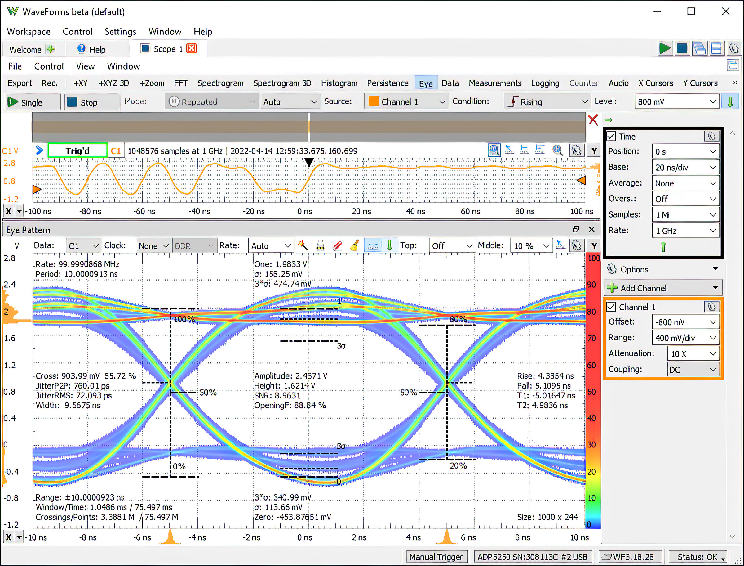
There are several other configuration choices as well, like averaging rate and threshold, the width in time of the eye, and more. The most useful is the “Show measurement” option, which overlays different measurements like the crossing points, the jitter, or the amplitude voltages onto the eye. Figure 4 shows an example of that.
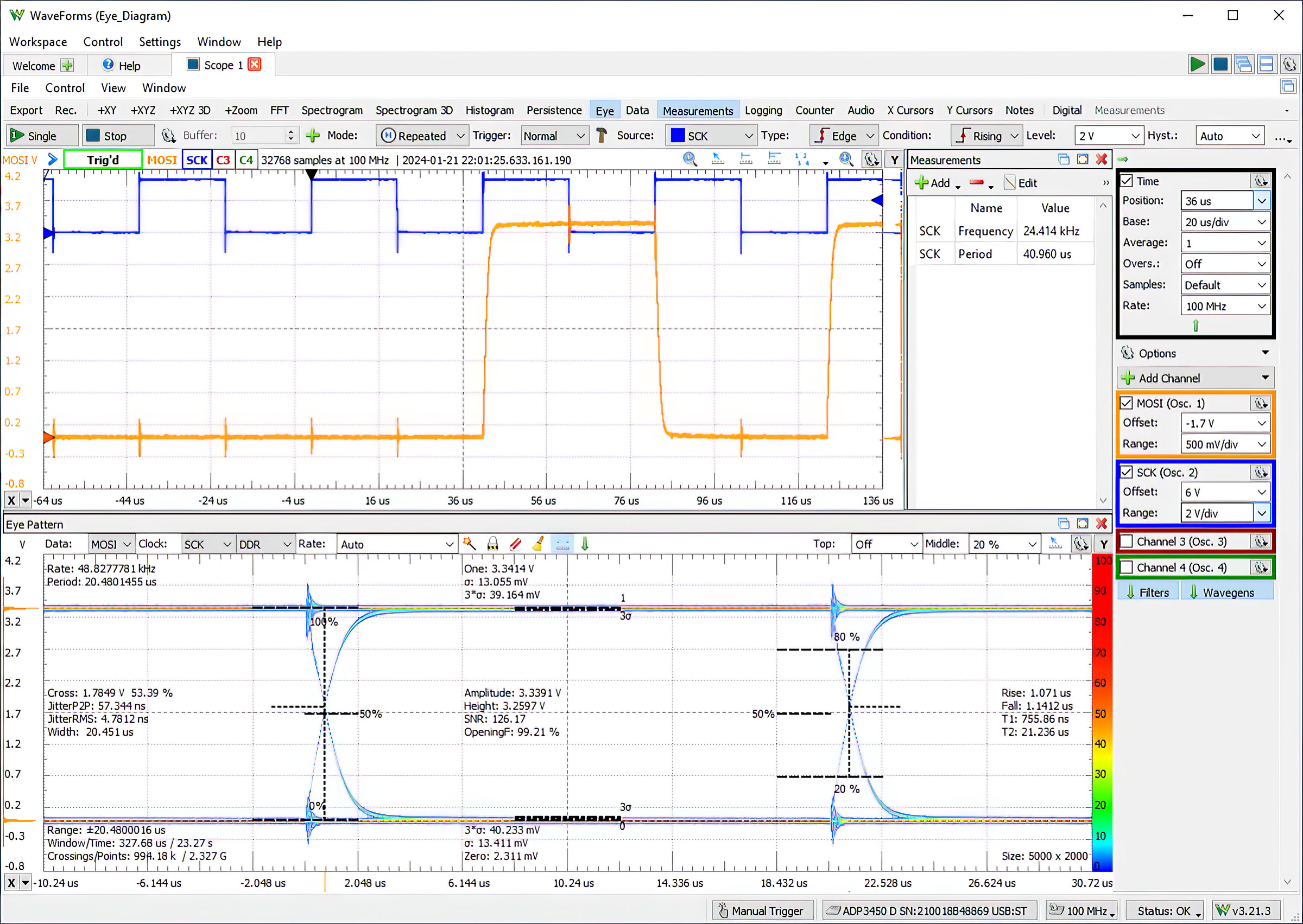
The bottom axis of the view shows the histogram of the crossing point, while the left axis displays the vertical histogram. The eye diagram in this example also reveals the (small) jitter of the data line and the ringing at the edge transitions.
WaveForms can also create an eye for transmissions without a clock signal by triggering on the data line in the “Eye” view. Figure 5 shows an example of such a setup with a heavily distorted signal.
Conclusion
Eye diagrams are a useful tool to quickly judge the quality of a transmission line in terms of jitter and anomalies. The right oscilloscope and the right software, like the ADP5250 together with WaveForms, make the generation of an eye diagram easy and fast.
Have not gone downstairs to check but can the AD3 do the eye diagram also?
Hi, downstairs now and the EYE tool is there so my question should be can the AD3 do eye diagrams and could you show how to setup the AD3 to do an eye pattern using something like a large SPI generated ourput from the the protocol tool and eye tool. I am sort of trying I got the scope up with the eye tool and told I need to use the protocol to send out a signal. Ok I’m not really good with the AD3 and would like to use it to see an eye diagram how the setup could be done with the AD3 to then move it on to a real project. Please don’t post this as I must look like a real idiot. Or my first post cause I was too lazy to rush downstairs to see if the EYE tool was on my Waveform.
Sorry for being a pain.