

 What’s the difference between the Pmod OD1 and the Pmod OC1? What’s the difference between an open drain output and an open collector output? What’s the difference between a MOSFET (metal-oxide field-effect transistor) and a BJT (bipolar junction transistor)? It turns out these are all essentially the same question! However, it can take some time to come to that realization, especially if new to understanding the different transistor technologies out there. To get to the answer, we’ll start with the last version of the question and work our way back through the first.
A Brief Overview of Transistors
BJT and MOSFET are two different types of transistors. They have similar functions, yet different characteristics. In terms of functionality, they can both be used as amplifiers or switches. As amplifiers, they take in a small current at one end and produce a much larger current out the other end. This is especially useful in analog circuits where transistors form the basis of components such as operational amplifiers.
As switches, a small current through one part of the transistor can switch on a larger current through another part of it. In other words, the transistor can be in two distinct states and represent two different values; 0 or 1, off or on. This is especially useful in digital circuits and is the foundation of how all computer chips work.
All transistors are made from silicon, an electrically neutral chemical element defined as a semiconductor, which means it is neither a great conductor of electricity nor a great insulator. What’s so useful about silicon is that its behavior can be altered in a known way by adding impurities, through a process called “doping.” If silicon is doped with certain chemicals, it gains extra “free” electrons and can more readily carry an electric current. This type of silicon is known as n-type, or negative type.
The opposite can also be done, creating p-type, or positive type, which has fewer free electrons and is often described as having holes where the electrons should be. Note, however, that neither n-type or p-type silicon is electrically charged. Therefore, they can be joined together and the electrons and holes will not begin to cross the n-p junction until an electrical current (BJT) or voltage (MOSFET) is applied. Different configurations of n-type and p-type silicon is what gives rise to the difference between BJTs and MOSFETs. (To learn further on transistors, check out Transistor Basics)
BJTs
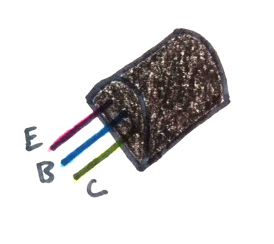
Bipolar junction transistors (BJT) are current-driven devices and come in two types, NPN and PNP. As the name suggests, NPN BJTs have two layers of n-type silicon surrounding one layer of p-type silicon (and vice-versa for PNP). Each layer has a specific name: the emitter, the base and the collector. See Figure 1.
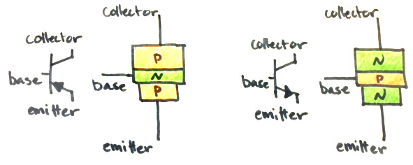
The operation principles behind each type of BJT are almost identical; the functional difference lies mainly in biasing of the junctions. For example, when positive bias is applied to the base of an NPN transistor, the device is turned on and current flows from the emitter to the collector. Also known as a low-side switch, the emitter connects to GND and the collector connects to the load. In contrast, when negative bias (or 0v/GND) is applied to the base of a PNP transistor, the device is turned on and current flows from the collector to the emitter, in the opposite direction from an NPN device. Also known as a high-side switch, the emitter connects to the voltage supply and the collector connects to the load.
In terms of pros and cons, BJTs are handy for driving low-power LEDs and similar devices from common microcontrollers that can only put out a DC voltage of 5 V, such as chipKIT and Arduino. Logic level MOSFETs can be used in the same way but are generally more expensive and harder to find than standard MOSFETS, which need 10 V or more to turn on. BJTs also switch faster than MOSFETs so are good for high-frequency applications, however they are less power efficient so are not always a great choice for battery-powered applications where the load is variable.
For more information on the theory behind BJTs, see this link, and for an enlightening animation, go here.
MOSFETs
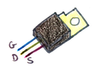
Metal-oxide field-effect transistors (MOSFET) are voltage driven devices and are like BJTs in that they have three different terminals: the source (analogous to the emitter), the drain (analogous to the collector), and the gate (analogous to the base). Also like BJTs, MOSFETs are comprised of n-type and p-type silicon, but they are arranged in a slightly different fashion. See Figure 3.
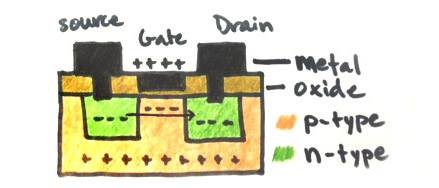
There are several sub-categories of MOSFET but the two I’ll mention here are N-channel and P-channel. The difference between the two lies in the applied voltage and what type of charge carrier is responsible for the flow of current. For an N-channel MOSFET, the source is connected to ground and the device is activated by applying a positive voltage to the gate. This creates an electric field, a “field-effect,” and allows electrons to flow in a thin channel from source to drain. For a P-channel MOSFET, the source is connected to Vcc and the device is activated by connecting the gate to ground. Here holes, instead of electrons, are the charge carrier. N-type MOSFETS are the most commonly used.
Note: Because only one type of charge (electron or hole) flows through a MOSFET, they are “unipolar” transistors as opposed to BJTs which allow both types of charge to move through the NP/PN junctions.
In terms of pros and cons, MOSFETs have infinitely high input impedance which makes them useful in power amplifiers. They are also more power efficient than BJTs and more tolerant to heat. Although BJTs can switch faster, MOSFETs are still fast enough for applications under 1 Mhz and are the most commonly used transistor today. In general, you can think high input impedance and low power consumption = MOSFET, and very high frequency operation and high current drive capability = BJT.
For more information on MOSFETs see this article.
What’s the difference between an open drain output and an open collector output?
After reading through the above sections, I’m sure you can guess as to the answer to this version of the question. If you said the difference is MOSFET vs BJT you’d be correct! An open drain or open collector output pin is simply a pin driven by a single transistor, either MOSFET or BJT respectively. In terms of uses, the answer mirrors the discussion above regarding pros and cons of MOSFETs and BJTs themselves. Of course, they can also be combined together to create very interesting circuits leveraging the strengths of each.
What’s the difference between the Pmod OD1 and the Pmod OC1?
Finally, we’re to the last form of the question, and again, the answer is now readily apparent. The Pmod OD1 is an open drain output module with four open drain output pins, each driven by an N-channel MOSFET. The Pmod OC1 is an open collector module with four open collector output pins, each driven by an NPN BJT. Both modules are used to sink higher current than what the pins on your Digilent FPGA or microcontroller can achieve.
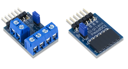
The Pmod OC1 was designed to drive slightly higher current devices at 200 mA, such as a small lamp or relay, and has a higher ESD rating than the Pmod OD1. Therefore, it is particularly robust and suited for students learning to use this circuit. It is rated for up to 20 V. The Pmod OD1 includes screw terminals on each pin and was designed specifically to drive stepper motors. However, it could also be used for many other high current applications up to 3 A. It is rated for up to 40 V.
For more information about the Pmod OD1 or the Pmod OC1, visit the Digilent wiki or leave a comment below!
References
How to Use MOSFET – Beginner’s Tutorial
How to Use BJT Bipolar Junction Transistor – Beginner’s Tutorial
Basics: Open Collector Outputs
Difference Between BJT and MOSFET
ES UN GRAN TRABAJO…..GREAT JOB