

Let’s talk about clocking. It’s crucial to the functionality of FPGA boards and digital design in general, as all synchronous logic depends on clocks. In this article, we’ll define some terms, briefly discuss the architecture of a 7-series CMT, and then preview a practical example of how we can mess around with an output clock, changing the frequency during runtime.
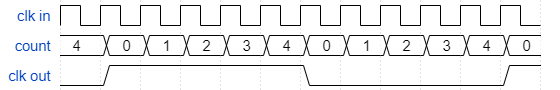
- Clock Dividers are a fundamental concept – a simple counter can be used to cleanly divide a clock. For example, counting from 0 – 4 and toggling divides a clock by 10 (as below). For routing reasons, it’s best to avoid implementing a true clock divider in an FPGA, but FPGAs still make use of built-in clock dividers.
- Voltage Controlled Oscillators (VCOs) are a programmable type of clock source – put simply, a specific voltage level applied to the input of a VCO produces a corresponding frequency. Changing that voltage level based on certain conditions thus changes the clock.
- Phase Frequency Detectors (PFDs) are used in conjunction with other signal conditioning circuitry to generate a signal for a VCO, by adjusting the frequency and phase until a clock fed back from its VCO matches a reference clock.
- Phase-Locked Loops (PLLs) and Mixed-Mode Clock Manager (MMCMs) are two similar architectures used in AMD FPGAs to take a reference clock and use it to consistently generate new clocks with various frequency and phase relationships to each other.
- Clock Buffers (BUFG, BUFR, etc) are a broad topic but generally are used to route clocks to and from different areas of an FPGA chip. As an aside, routing was mentioned earlier, and is a huge topic that this post won’t get into. Perhaps another time.
- Clock Management Tiles (CMTs) are the name that AMD uses for hardware built into their FPGAs’ that is dedicated to clocking. On 7-series parts, like those commonly used on our FPGA boards, these consist of an MMCM and a PLL.
It should be said, that while most of this is critical information for complex projects, AMD provides an IP called the Clocking Wizard, which automatically handles much of the configuration of CMTs in your projects – new users need not fear (at least keep the fear to a healthy level).
For extensive detail on clocking resources available in 7 series parts, check out UG472 – 7 Series Clocking
To break down a 7-series MMCM, take a look at this diagram from UG472:
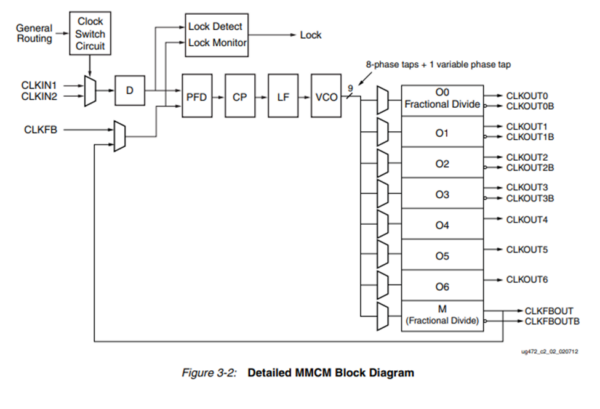
A clock input is passed to an MMCM and can then be divided down (block “D”). Alongside a feedback clock, this clock is passed into a PFD. When combined with another clock divider between the VCO and feedback, this functionally lets us multiply the input clock by a programmable value. Additional fractional divide stages for each of the other clock outputs let us generate a wide variety of different frequencies with one CMT at the same time.
Functionally, the frequency of any particular output clock can be expressed as the frequency of the input clock, divided by a single programmable constant, multiplied by a fractional value, and then divided again by another fractional value:
- FVCO = FCLKIN1 * CLKFBOUT_MULT / DIVCLK_DIVIDE
- FCLKOUT1 = FVCO / CLKOUT#_DIVIDE
Where the following are values that can be set in programmable registers:
- CLKFBOUT_MULT – the feedback clock multiplier – is a fractional number with 8-bit integer component (0-255) and fractional component ranging from 0.000 to 0.999. Used in block “M”, above.
- DIVCLK_DIVIDE is an 8-bit integer in range 0-255, the value used in clock divider “D”, above.
- CLKOUT#_DIVIDE is a fractional number with 8-bit integer component (0-255) and fractional component ranging from 0.000 to 0.999. Each output clock’s divider (blocks O0-O6) can be separately programmed.
Not all combinations of values that can be programmed into registers result in valid clocks that can actually run in an FPGA. AC/DC switching characteristics documents for each AMD FPGA family, like DS189, specify minimum and maximum frequencies for each device. For example, MMCM_FVCOMAX, the maximum VCO output frequency, for Spartan-7 speed grade -1 parts, like the one found on the Arty S7-50, is 1200 MHz. The settings that produce good clocks can be pretty narrow – for a full description of the process of picking values that will work, check out the “MMCM/PLL Programming” section of UG472.
We won’t get into it here, but phases are similarly programmable. Note that the “Phase Duty Cycle Config” setting in the Clocking Wizard’s Clocking Options tab needs to be checked to be able to reprogram clock phases and duty cycles.
In an upcoming blog post, we’ll be putting some of these resources to the test. We created a testbed that allows for automatic control of a clock, by exposing the AXI4-Lite interface of a Clocking Wizard to a serial port. This allows us to read and write its registers from a host computer, remotely changing the frequencies and phases of the clocks that the CMT is outputting. These clocks are used to drive several registers, whose outputs are directed to Pmod ports so that they can be viewed on an oscilloscope. Sources for the testbed, built for our Arty S7-50 FPGA development board, are now available on our GitHub, described on this reference page: Arty S7-50 Clocking Wizard Testbed
Its architecture is roughly as follows:
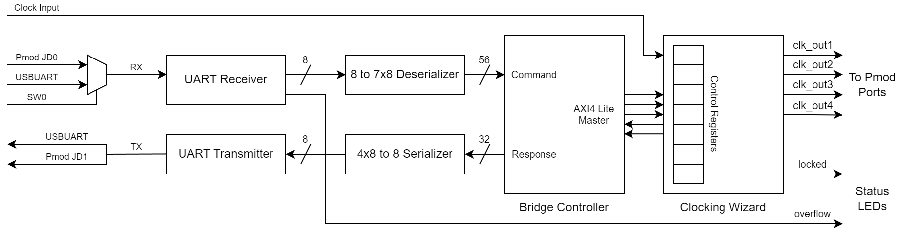
Commands are received from a PC via UART, either from a Pmod pin or from USBUART. They consist of a single “r”ead or “w”rite byte, two address bytes, and four data bytes. Once a command has been collected, a custom controller translates these commands into AXI4-Lite transactions with the Clocking Wizard, potentially setting some register’s value or returning some data back to the host. Some example commands are shown in a Python script, which can also be found through the reference page, used to control the USBUART serial port. More info on the Clocking Wizard’s address space and register map can be found in AMD’s product guide for the IP, [Clocking Wizard LogiCORE IP Product Guide PG065. It should be noted that since toggling registers are used at the outputs, frequencies of signals output by this testbed are divided down by a factor of two further than the MMCM outputs described above – expected phase differences between edges are also affected!
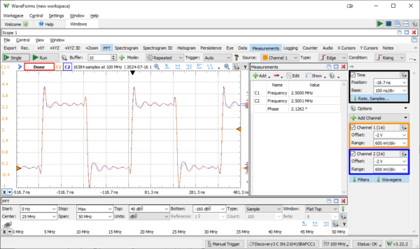
For a quick sample of what a clock output looks like, complete with frequency and phase offset measurements, this screenshot was captured using an Analog Discovery 3. Note the substantial overshoot in clock edges – this could be due to the use of flywires for analog input, and properly-compensated BNC scope probes could help.
Stay tuned for some captures of these clock signals with a higher-bandwidth scope!