

At Digilent, we believe in the power of community. Our forums are a hub where users come together to share knowledge, ask questions, and find solutions to their design challenges. This blog post highlights a recent interaction on our forum.
Read the full forum thread here: Arty-A7 series ddr3_reset_n uses incorrect standard SSTL135 – FPGA – Digilent Forum
The Challenge
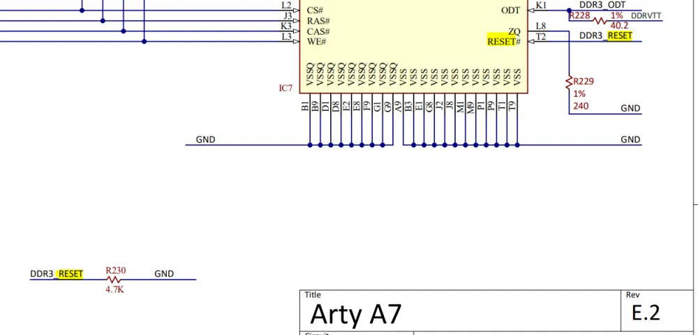
Circuit simulations – especially when easily sharable over the internet – are a key piece of clear communication around electrical engineering. When a Digilent community member reached out on our forum to inquire about how exactly the DDR reset pin on the Arty A7 FPGA board works, one of Digilent’s support engineers put together a circuit simulation in Multisim Live to help explain the details.
Forum User: As you can see from this simple analysis, if the FPGA DDR3 reset output is configured for SSTL135, then the reset logic level will be invalid at the DDR3 device.
The easy solution would be to set the FPGA IOSTANDARD to LVCMOS135 … but no such standard is accepted in Vivado. Using LVCMOS12 or LVCMOS15 results in an error.
This seems like a limitation of Vivado more than the Digilent board design, since the VCCO band in which you want to generate the reset signal should be a 1.35V bank, but then there is no LVCMOS standard that is acceptable to the tool (I am testing using v2024.1).
Can Digilent please provide some insight into their design?
The Solution
In brief, the electrical characteristics of the input and output pins used, in combination with a pulldown resistor, make the Arty’s reset pin function exactly as necessary, despite what might seem at first glance to be a non-standard design. An SSTL interface normally drives a circuit with substantial termination resistors and drives an output by pulling it to either ground or a power rail. The effective resistance between the power rail and the output is small enough that the resistance of a high impedance CMOS input or even a small pulldown resistor isn’t enough to overcome the drive strength of the output. Input and output threshold specifications normally only used when SSTL outputs drive SSTL inputs confuse the picture, but with a proper understanding of the actual electrical characteristics, and a simulation to prove it out, the real-world behavior falls through.
The Role of the Pulldown Resistor
That resistor might also look redundant, but it plays an important role in pulling the reset low when the FPGA isn’t configured – making sure the memory is held in reset until the FPGA is ready to use it.
Digilent Support
The Digilent team is committed to providing expert assistance and guidance to its customers. By sharing knowledge and working together, users can overcome even the most challenging design problems. We encourage you to join our community and participate in discussions with other engineers and enthusiasts.
Read the full forum thread here: Arty-A7 series ddr3_reset_n uses incorrect standard SSTL135 – FPGA – Digilent Forum