

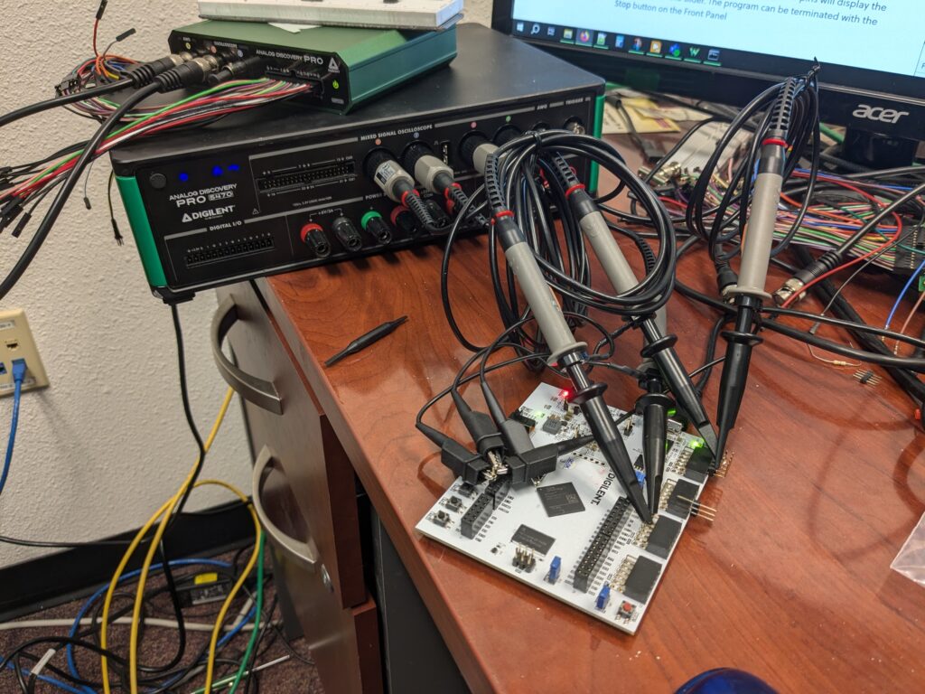
Digilent recently announced the release of two new members of the Analog Discovery Pro 5000 Series, the ADP5470 and ADP5490, which are both four-channel mixed-signal oscilloscopes offering substantially higher bandwidths and sample rates than any comparable oscilloscope Digilent has previously released. In this article, we will take advantage of those bandwidths to perform some testing on an FPGA board.
In the FPGA world, a frequently asked question is exactly how fast a pin can be toggled, as it directly informs the maximum speed at which data can be transferred onto or off of a board. This maximum speed depends on many factors, including the length of PCB traces between connector and FPGA pin, the presence (or lack thereof) of current-limiting protection resistors, and the inherent quality of a connector used. Pmod connectors are easier to use and to design peripherals for than other commonly used connectors, like SYZYGY or FMC, but signals run through them can only achieve limited speeds.
So, I put together a project that toggles the Pmod I/O pins on an Arty S7 at controllable frequency, by exposing Clocking Wizard register settings through a simple command interface connected to a serial port. In this way, the serial port can be controlled from a Python script to consistently configure the clock while also recording clock pulses using an ADP5490. This post is focused on the ADP5000 devices, so the details of the Arty S7 project are out of scope (pun intended) for this article, but a post we put out a couple of weeks ago covers it in more detail: VCOs, MMCMs, PLLs, and CMTs – Clocking Resources on FPGA Boards.
For a digital signal to be properly transmitted from one device to another, the output signal must exceed VOH and fall below VOL. For 3.3V LVCMOS logic, as is commonly used on our FPGA boards, for example, to count as a rising edge, a signal must transition from below 0.4 V to above 2.4 V.
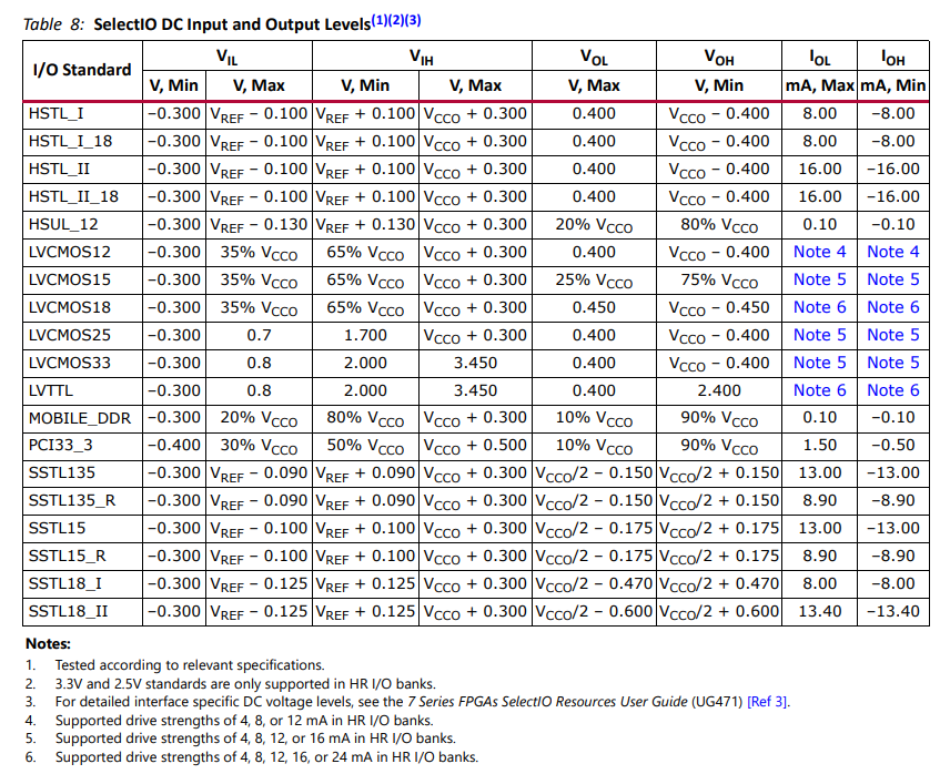
Table 8, SelectIO DC Input and Output Levels, from DS189, Spartan 7 AC/DC Switching Characteristics, describes the logic thresholds for various logic standards. Note that these values are defined for DC signals, and whether or not they can be achieved when the pin is toggling quickly and the chip is placed on a PCB depends on the analog characteristics of the board – which we’re about to test.
By observing increasing frequencies of clock signal with the scope, we can see that the LVCMOS33 voltage levels are no longer met once the clock is run faster than [unknown frequency].
WaveForms’ cursors feature makes it easy to spot things like “Does this signal rise above this threshold?” at a glance. In the screenshots you’re about to see, we placed cursors, the red lines, at a couple of common threshold voltage levels, so that we could confirm whether our output signals met the spec.
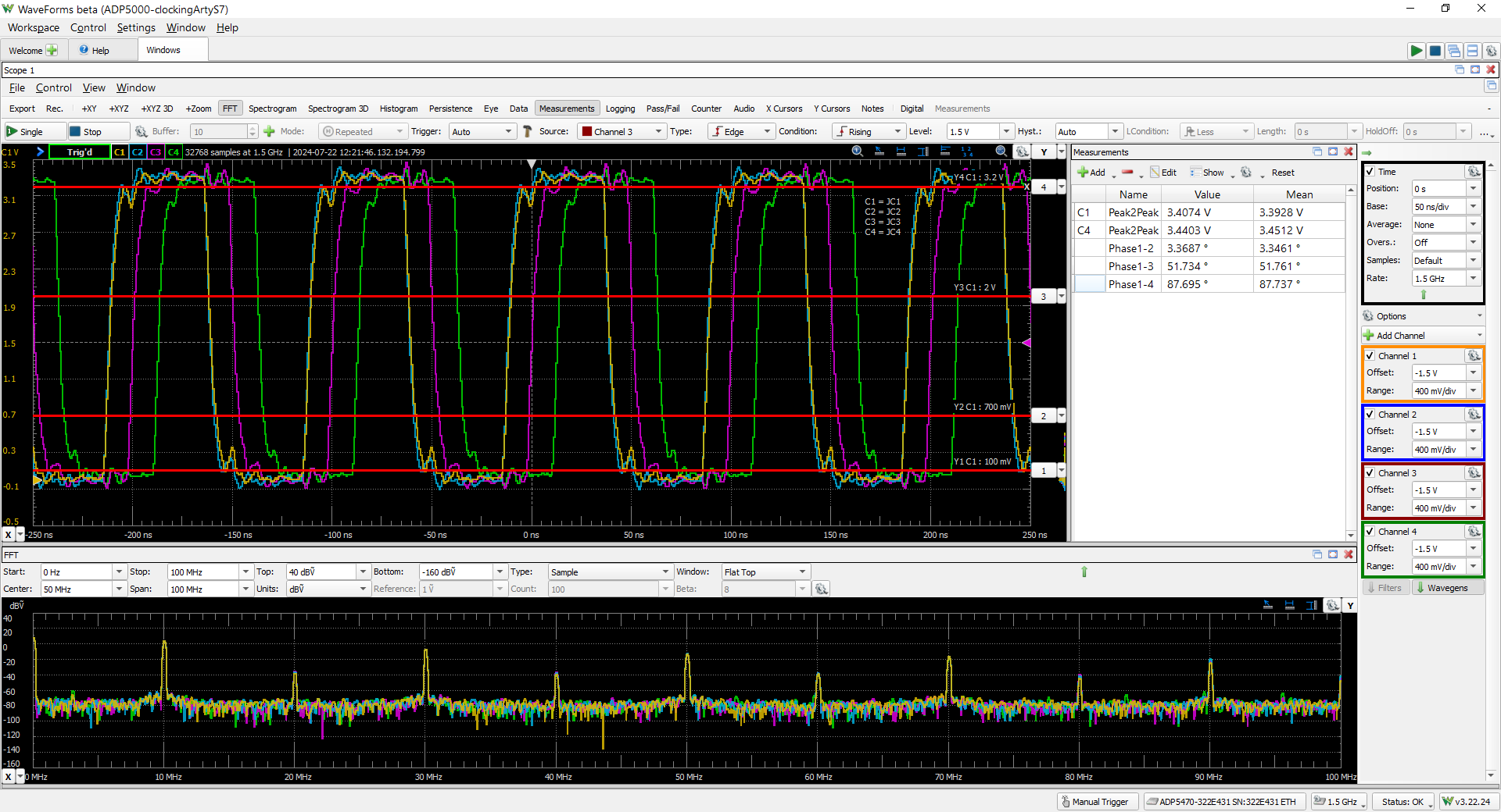
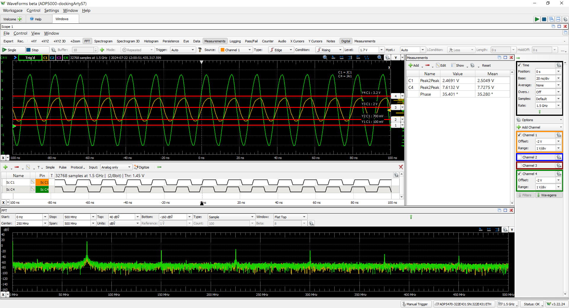
Output signals with varying phase shifts relative to each other, 10 MHz. Expected phase shifts are ~0 degrees between C1 and C2, 45 degrees between C1 and C3, and 90 degrees between C1 and C4. We can see that these are pretty close.
Note, the cursors we used in these tests don’t match the thresholds outlined by AMD above.
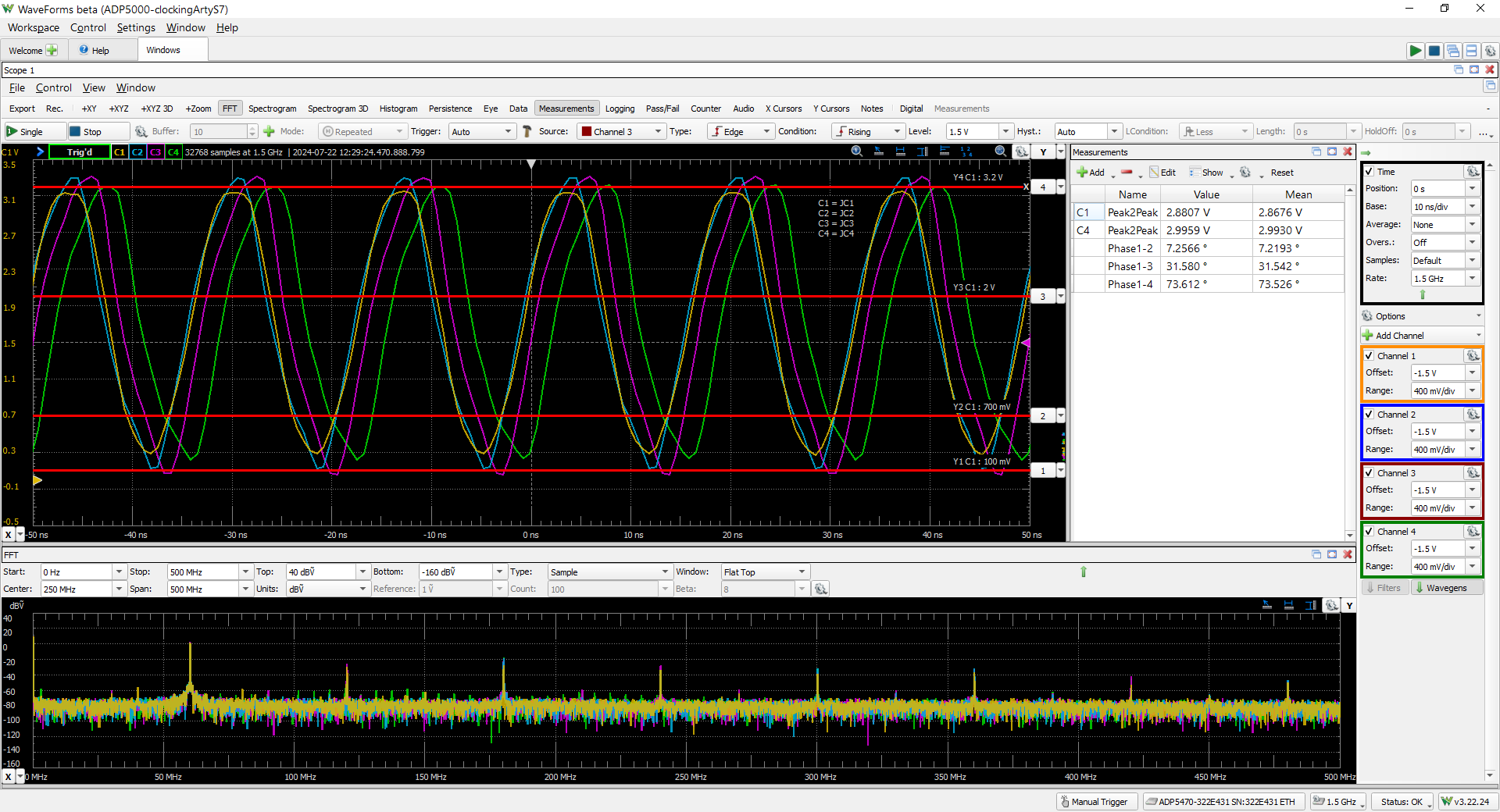
The same clocks at 60 MHz – slew rates begin to matter, though it can be seen that thresholds are still respected. Note that harmonics are still present, even if they have less impact on the shape of the square wave edges. You can see here that we’re capturing multiple different harmonics of these waves, all the way up to the 7th at 420 MHz.
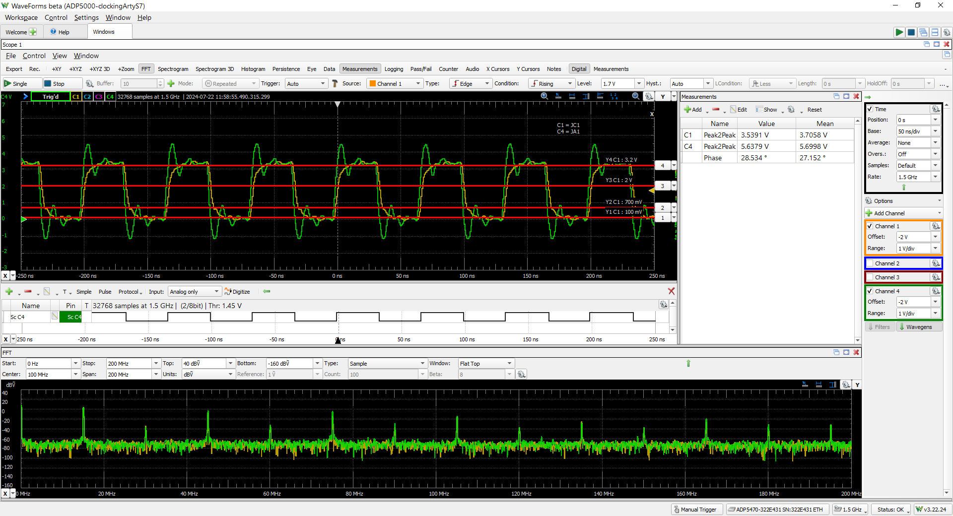
Things can get funky at high frequencies. Here we see a 75 MHz output, which, while it seems to be able to keep up and swing past the thresholds, also seems to have a much higher amplitude than expected. A smoothed-out overshoot?
To really get a sense of differences that can occur due to hardware outside of the FPGA part, let’s look at this 15 MHz signal, comparing the JC1 and JA1 outputs. One of these has a series resistor while the other doesn’t. As a side note, the Scope to Digital feature, which allows us to interpret analog signals in a logic analyzer-style view, with an adjustable threshold, is also extremely useful for this kind of testing.
While it’s been extremely useful in debugging FPGA projects, my AD3 doesn’t have the input bandwidth to cover the frequency range necessary for this kind of test – necessitating the bigger scope. As to why, an FFT view of the clock signal – seen in all of the screenshots above – shows us an important property of square waves, namely, their many harmonic frequencies, which can impact the quality of a clock edge. An oscilloscope may need to capture many of these harmonics to properly reflect the signal as it’s seen by a device it’s driving, at many times the “base” frequency of the signal in question.
I need to add one big caveat: All of this testing was done with one specific board and project, with no external circuit other than the oscilloscope connected to the I/Os. Results would be different as soon as a Pmod was connected to a Pmod port. So your mileage may vary.
If you’re interested in these topics, you might also like this post that we put out on Eye Diagrams in WaveForms, or this older article on generating near-square waves by composing them from harmonics in a custom waveform: Using the Analog Discovery 2 to Measure Harmonics in a Signal.
Check out the Analog Discovery Pro 5000 Series page on our store, where you can find more reference material and information on their specifications.