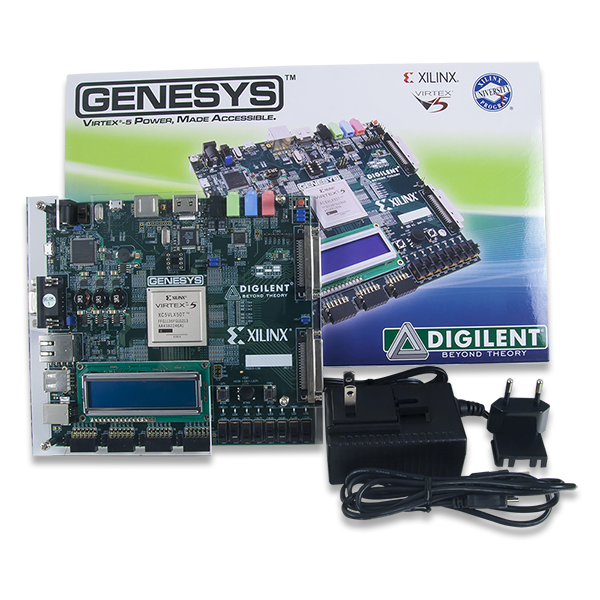
Genesys
Reference Manual
Technical Support
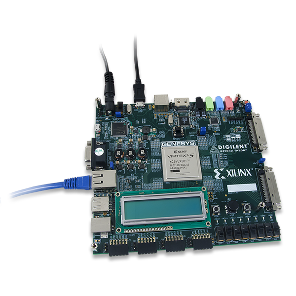
Genesys
Virtex-5 FPGA Development Board
Features
- Multiple USB2 ports for programming, data transfer, and hosting applications
Key Specifications
Memory
16Mbyte StrataFlash™ for
configuration and data storage
configuration and data storage
Logic Cells
7,200 slices (4 LUTs and 8 flip-flops)
Block RAM
1.7Mbits
DCM
12
PLL
6
DSP
48 slices
Internal clock
500MHz+
DDR2
256MB DDR2 SODIMM with
64-bit wide data
64-bit wide data
Ethernet
10/100/100 PHY and
RS-232 serial port
RS-232 serial port
Connectivity and On-board I/O
HDMI
Up to 1600×1200 and 24-bit color
Audio
AC-97 Codec with line-in,
line-out, and headphone
line-out, and headphone
Pmod Connectors
4
Connectors
112 I/Os routed
to expansion connectors
to expansion connectors
Switches
1 2-axis navigation switch
8 slide switches
8 slide switches
LCD
16×2 character
Buttons
2
LEDs
8
Electrical
Power
5V external (2.1mm coaxial) supply
Logic Level
3.3V
Physical
Width
x in
Length
y in
Note:
The Genesys is no longer available. Please see the Genesys 2 as an alternative to this product.
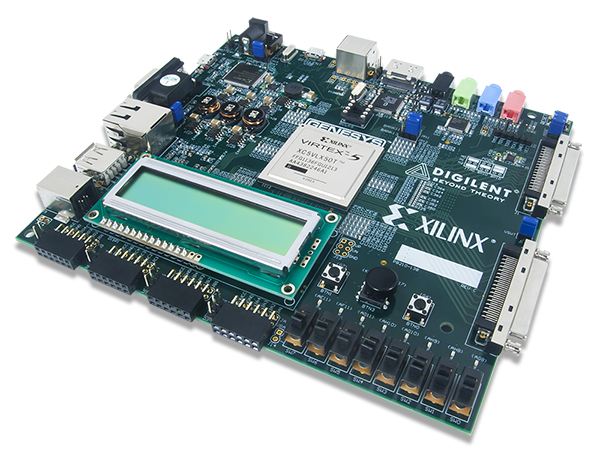
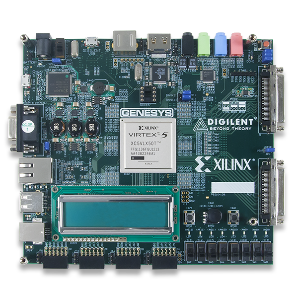
The Genesys circuit board is a complete, ready-to-use digital circuit development platform based on a Xilinx Virtex 5 LX50T. The large on-board collection of high-end peripherals, including Gbit Ethernet, HDMI Video, 64-bit DDR2 memory array, and audio and USB ports make the Genesys board an ideal host for complete digital systems, including embedded processor designs based on Xilinx’s MicroBlaze. Genesys is compatible with all Xilinx CAD tools, including ChipScope, EDK, and the free WebPack, so designs can be completed at no extra cost.
Tutorials
Example Projects
Additional Resources
- Ethernet Project Download
- Ethernet demonstration project (LightWeight IP demonstration project originally for Xilinx ML505 ported to Genesys).
- Microblaze EDK DemoDownload
- This zip file contains an EDK demo project that illustrates how to use the Genesys AC97 codec with Microblaze.
- EDK BSB ProjectDownload
- Tutorial and example project showing a Genesys-based design, generated with the EDK BSB wizard.
- EDK and SDK Projects Download
- A Microblaze based audio demo that demonstrates how to use the AC97 audio codec.
- Out of Box Demo/Test Download
- The source code for the out of box demo and test the exercises all onboard components. This is a very advanced Microblaze project and the source code for it may be difficult to follow, but it is useful to teach advanced users how to use specific components.