Table of Contents
Current and Power Adapter Reference Manual
The Current and Power Adapter helps you visualize currents, voltages, and powers in a DC or AC circuit. The Adapter is inserted between the power source and the load and uses Analog Discovery and the WaveForms software to perform calculations on the circuit.


Overview
Features
- Uses a low value shunt resistor
- Allows Current and Voltage range scaling
- Compatible with the Analog Discovery 3, Analog Discovery 2, and Analog Discovery (Legacy)
Compatible Products
The Current and Power Adapter is compatible with the following:
- Analog Discovery (Legacy)
Note: Banana cables are not included with the Current and Power Adapter
About this Document
This reference manual applies to Revision B.2 of the Current and Power Adapter.
Software Support
The Analog Discovery Current and Power Adapter is controlled with the Analog Discovery 3 through the use of WaveForms.
Functional Description
Connectors and Jumpers
| Label | Name | Description |
|---|---|---|
| J1 | Power Source Input | Used to as the input of the external power source to the Adapter |
| J2 | Ground Connection | Used to establish a common ground between the power source, adapter, and external load |
| J3 | Adapter output | Used to connect the Adapter to the external load |
| J4 | 2×15 MTE connector | Connects the Current and Power Adapter to the Analog Discovery |
Warning: The J2 GND connector connects the Adapter to the reference system ground. This is the GND of the USB interface, which further connects to the GND of the host computer. No voltage applied in the J1 or J3 binding posts can be beyond +/-40V relative to GND.
Measuring the Voltage and Current
The Analog Discovery Current and Power Adapter is used to visualize and measure Voltage and Current and compute Power transmission between a source and a load. It uses a 10 mΩ shunt resistor, a programmable gain current sense amplifier, as shown in the schematic diagram, CurrentPowerAdapter_sch.PDF. It also uses features of the Analog Discovery and WaveForms, as explained below:
- The Positive Voltage Supply to provide the 5V supply to the current sense amplifier.
- DIO9 (Gain1) and DIO8 (Gain2) to set the gain of the current sense amplifier.
- The Oscilloscope differential channels:
- Channel 1 to measure the Voltage between the poles of the Output binding post.
- Channel 2 to measure the output of the current sense amplifier.
Caution!
Take care to ensure that signals measured fall within specified input ranges and do not exceed the specified overvoltage protection range. Do not use the Current and Power Adapter for measurements within Measurement Categories II, III, or IV. For example, do not use the adapter to perform measurements on circuits directly connected to a standard wall outlet, building installations like circuit breakers, or power lines.
Hardware Structure and Equations
All equations and calculations in this document provided by Mircea Dabacan, PhD, Technical University of Cluj-Napoca Romania
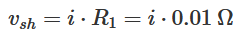
As seen in the schematic diagram, CurrentPowerAdapter_sch.PDF, the current flowing from In+ to Out+ poles generates a voltage across the shunt resistor R1:
Divided by R2, R3:

And amplified by the current sense amplifier:

The overall transfer function of the current stage is:
![]()
The current sense amplifier output voltage range is limited by the supply voltage minus 0.1 V rail margin:

The differential inputs of the channel 2 get the voltages:

The voltage shown by the C2 Scope signal is:

The gains and ranges are:
| DIO8 | 0 | 0 | 1 | 1 |
| DIO9 | 0 | 1 | 0 | 1 |
| G | 10 | 20 | 50 | 100 |
| i | -25 A…+25 A | -12.5 A…+12.5 A | -5 A…+5 A | -2.5 A…+2.5 A |
| $v_{sh}$ | -250 mV…+250 mV | -125 mV…+125 mV | -50 mV…+50 mV | -25 mV…+25 mV |
| $v_{inCs}$ | -240 mV…+240 mV | -120 mV…+120 mV | -48 mV…+48 mV | -24 mV…+24 mV |
| $v_{C2}$ | -2.4 V…+2.4 V | -2.4 V…+2.4 V | -2.4 V…+2.4 V | -2.4 V…+2.4 V |
Current and Power Adapter Specifications
The Analog Discovery Current and Power Adapter uses the analog inputs of the connected Analog Discovery device and Scope instrument for measurements. Therefore, all of the specifications of the attached hardware affect the Current and Power Adapter specifications.
The Voltage measurements are directly done by the Analog Discovery scope channel 1, with all the respective features, errors, and limitations. The only additional limitation is due to the current sense amplifier which limits the minimum safe voltage of the Out+ binding post to -42 V relative to GND.
The Current measurements are done by the current sense amplifier (MAX49925), the sense resistor (1% tolerance) and five more resistors (0.1%). The signal is visualized with the Scope channel 2, set on low voltage range (500 mV/div or lower). The errors and limitations of these combine for the final specifications.
The power measurements are WaveForms computations of Voltage and Current acquired data. Except for arithmetic approximations, they do not introduce new errors.
All the specs below show typical values when used with an Analog Discovery 3.
| Input Type | Differential |
|---|---|
| Input Range | ±2.5 V with respect to ground (5 V peak-to-peak) |
| ±25 V with respect to ground (50 V peak-to-peak) | |
| Resolution | 14 bits (16-bit with averaging) |
| Absolute Resolution | 0.336 mV (scale ≤ 0.5 V/div |
| 3.36 mV (scale > 0.5 V/div) | |
| Accuracy | ±10 mV ± 0.5% (scale ≤ 0.5 V/div, VinCM = 0 V) |
| ±100 mV ± 0.5% (scale > 0.5 V/div, VinCM = 0 V) | |
| Bandwidth | 9 MHz @ -3 dB, 2.9 MHz @ -0.5 dB, 0.8 MHz @ -0.1 dB |
| Input Impedance | 1 MΩ ││ 24 pF |
| Input Coupling | DC |
| Vertical Sensitivity (range) | 200 µV/div to 5 V/div |
| CMMR | ±0.5% (typical) |
| Acquisition Modes | average, decimate, min/max, record |
| Overvoltage Protection | ±40 V instantaneous |
| Input Type | Differential |
|---|---|
| Input Range | ±2.5 A, ±5 A, ±12.5 A, ±25 A peak, selectable |
| Resolution | 14 bits (16-bit with averaging) |
| Absolute Resolution | 0.35 mA @ 2.5 A, 0.7 mA @ 5 A, 1.75 mA @ 12.5 A, 3.5 mA @ 25 A |
| Accuracy | ±1% of Full Scale |
| Bandwidth | 100 kHz @ 2.5 A, 200 kHz @ 5 A, 400 kHz @ 12.5 A, 600 kHz @ 25 A |
| Input Impedance | 10 mΩ |
| Input Coupling | DC |
| Vertical Sensitivity (range) | 200 µA/div to 5 A/div |
| CMMR | ±5 mA/V (typical) |
| Acquisition Modes | average, decimate, min/max, record |
| Overvoltage Protection | ±40 V peak |
Additional Information
All equations and calculations in this document provided by Mircea Dabacan, PhD, Technical University of Cluj-Napoca Romania
- For more information on the Current and Power Adapter and Analog Discovery 3, check out their resource centers: Current and Power Adapter, Analog Discovery 3
- WaveForms can be downloaded from the WaveForms Resource Center.