Table of Contents
Pmod CAN Reference Manual
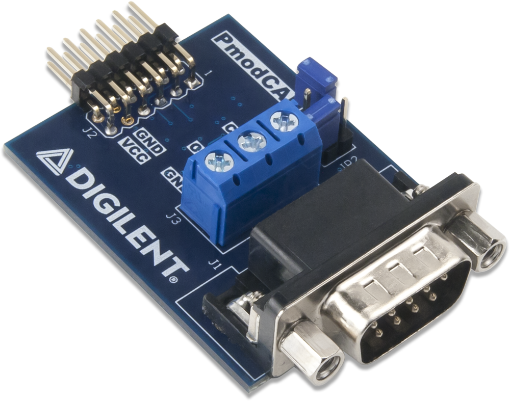
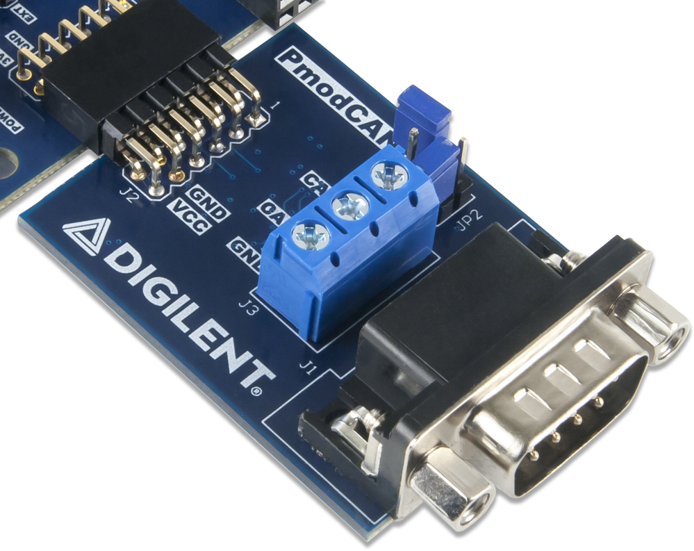
The Digilent Pmod CAN (Revision B) is a CAN 2.0B controller with an integrated transceiver. The embedded Microchip MCP25625 chip connects directly to the physical CAN bus and meets automotive requirements for high-speed (1 Mb/s), low quiescent current, electromagnetic compatibility, and electrostatic discharge.
Download This Reference Manual
Features
- Standalone CAN 2.0B controller with an integrated CAN transceiver
- Compatible with ISO-11898-1, ISO-11898-2, and ISO-11898-5
- Suitable for automotive applications
- Up to 1 Mb/s operation
- Up to 10 MHz SPI clock speed
- 3 Transmit buffers with prioritization and abort feature
- 2 Receive buffers
- 6 Filters and 2 masks with optional filtering on the first two data bytes
- Interrupt output pin
- Standard DB9 connector for a secure connection
- Suitable for 12 V and 24 V systems
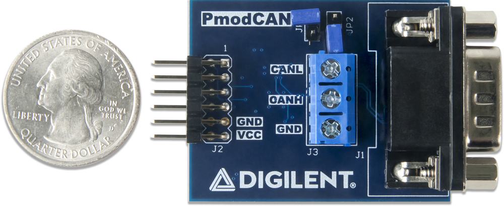
- Small PCB size for flexible designs 1.4 in x 1.8 in (3.6 cm x 4.6 cm)
- 12-pin Pmod connector with SPI interface
- Follows the Digilent Pmod Interface Specification 1.1.0
Specifications
| Parameter | Min | Typical | Max | Units |
|---|---|---|---|---|
| Power Supply Voltage (Vcc) | 2.7 | 5.5 | V | |
| High-Level Input Voltage (RxCAN) | 2 | - | Vcc+1 | V |
| Low-Level Input Voltage (RxCAN) | -0.3 | - | 0.15*Vcc | V |
| High-Level Output Voltage (TxCAN) | Vcc-0.7 | - | - | V |
| Low-Level Output Voltage (TxCAN) | - | - | 0.6 | V |
| Bit Frequency | 14.4 | - | 1000 | kHz |
| Transmitter | Min | Typ | Max | Units |
| Recessive Bus Output Voltage (CANH & CANL) | 2.0 | 0.5 Vcc | 3.0 | V |
| Dominant Output Voltage (CANH) | 2.75 | 3.50 | 4.50 | V |
| Dominant Output Voltage (CANL) | 0.50 | 1.50 | 2.25 | V |
| Dominant Differential Output Voltage | 1.5 | 2.0 | 3.0 | V |
| Receiver | Min | Typ | Max | Units |
| Recessive Differential Input Voltage (normal mode) | -1.0 | - | +0.5 | V |
| Dominant Differential Input Voltage (normal mode) | 0.9 | - | Vcc | |
| Parameter | Value | Units | ||
| Standby Current | 10 | μA | ||
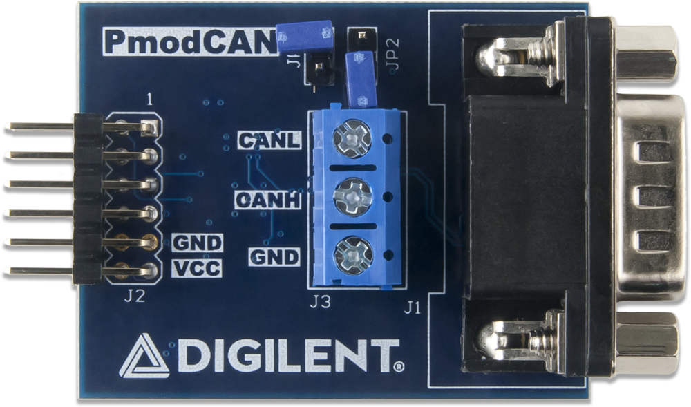
Pinout Table Diagram
| Header J2 | Header J1 | Header J3 | ||||||||||||
|---|---|---|---|---|---|---|---|---|---|---|---|---|---|---|
| Pin | Signal | Description | Pin | Signal | Description | Pin | Signal | Description | Pin | Signal | Description | Pin | Signal | Description |
| 1 | CS | Chip Select | 7 | INT | Interrupt | 1 | N/C | Not Connected | 7 | CANH | CAN High-Level Voltage I/O | 1 | CANL | CAN Low-Level Voltage I/O |
| 2 | MOSI | Master-Out-Slave-In | 8 | RST | Reset | 2 | CANL | CAN Low-Level Voltage I/O | 8 | N/C | Not Connected | 2 | CANH | CAN High-Level Voltage I/O |
| 3 | MISO | Master-In-Slave-Out | 9 | Rx0BF | Receive Buffer 0 Full Interrupt | 3 | GND | Power Supply Ground | 9 | N/C | Not Connected | 3 | GND | Power Supply Ground |
| 4 | SCK | Serial Clock | 10 | Rx1BF | Receive Buffer 0 Full Interrupt | 4 | N/C | Not Connected | S1 | GND | Power Supply Ground | Jumpers | ||
| 5 | GND | Power Supply Ground | 11 | GND | Power Supply Ground | 5 | N/C | Not Connected | S2 | GND | Power Supply Ground | JP1 | Loaded/ Unloaded | End of bus terminated with a combined 120Ω impedance/ Do not terminate the end of the bus |
| 6 | VCC | Power Supply (3.3V) | 12 | VCC | Power Supply (3.3V) | 6 | GND | Power Supply Ground | JP2 | Loaded/ Unloaded | Terminate the CAN bus lines with a capacitor to ground/ No termination | |||
Physical Dimensions
The pins on the pin header are spaced 100 mil apart. The PCB is 1.8 inches long on the sides parallel to the pins on the pin header and 1.4 inches long on the sides perpendicular to the pin header.
Functional Description
The Pmod CAN utilizes the Microchip MCP25625 to enable CAN communication with a variety of external devices. A complete CAN solution with a controller and transceiver can be implemented on a system board by communicating with the host board via the SPI protocol in SPI mode 0 or 3. The two differential lines on the transceiver, CANH and CANL, enable balanced differential signaling to eliminate most of the electromagnetic field (EMF) and provide high noise immunity within the system.
Serial Communication
The Pmod CAN communicates with the host board via the SPI protocol. By driving and keeping the Chip Select line (pin 1) at a logic level low, users may communicate back and forth with the Pmod depending on whether or not both sets of data lines are enabled. The embedded chip on the Pmod operates in SPI Mode 0 or 3, with data captured on the rising edge of the clock and data transferred on the falling edge of the clock, and a minimum clock cycle time of 100 nanoseconds as per Table 7-6 (page 70) of the Microchip MCP25625 datasheet.
Nine SPI instructions are available to read the status of the receiver, load a transmit buffer, modify bits in a register and more. Most of the instruction commands are single byte instructions followed by an address byte. More information is available in the Quick Start section as well as Section 5 (page 55) of the MCP25625 datasheet.
Register Details
CANINTE
The CANINTE register (page 51) enables the generation of interrupts on Pin 7.
| CANINTE 0x2B | ||||
|---|---|---|---|---|
| Bit Name | Bit Number | Bit Description | Bit Values | Functional Description |
| MERRE | [7] | Message Error Interrupt Enable Bit | 0¹ | 1-Interrupt on error during message reception or transmission/0-Disabled |
| WAKIE | [6] | Wake-up Interrupt Enable Bit | 0¹ | 1-Interrupt on CAN bus activity/0-Disabled |
| ERRIE | [5] | Error Interrupt Enable Bit | 0¹ | 1-Interrupt on EFLG error condition change/0-Disabled |
| TX2IE | [4] | Transmit Buffer 2 Empty Interrupt Enable Bit | 0¹ | 1-Interrupt on TXB2 becoming empty/0-Disabled |
| TX1IE | [3] | Transmit Buffer 1 Empty Interrupt Enable Bit | 0¹ | 1-Interrupt on TXB1 becoming empty/0-Disabled |
| TX0IE | [2] | Transmit Buffer 0 Empty Interrupt Enable Bit | 0¹ | 1-Interrupt on TXB0 becoming empty/0-Disabled |
| RX1IE | [1] | Receive Buffer 1 Full Interrupt Enable Bit | 0¹ | 1-Interrupt when message received in RXB1/0-Disabled |
| RX0IE | [0] | Receive Buffer 0 Full Interrupt Enable Bit | 0¹ | 1-Interrupt when message received in RXB0/0-Disabled |
¹ – This is the default value on power-up or reset
CANINTF
The CANINTF register (page 52) holds the flags of all the interrupts that are enabled through the CANINTE register. If an interrupt flag is set, it must be cleared by the system board to reset the interrupt condition.
| CANINTF 0x2C | ||||
|---|---|---|---|---|
| Bit Name | Bit Number | Bit Description | Bit Values | Functional Description |
| MERRF | [7] | Message Error Interrupt Flag Bit | 0¹ | 1-Interrupt pending/0-No interrupt pending |
| WAKIF | [6] | Wake-up Interrupt Flag Bit | 0¹ | 1-Interrupt pending/0-No interrupt pending |
| ERRIF | [5] | Error Interrupt Flag Bit | 0¹ | 1-Interrupt pending/0-No interrupt pending |
| TX2IF | [4] | Transmit Buffer 2 Empty Interrupt Flag Bit | 0¹ | 1-Interrupt pending/0-No interrupt pending |
| TX1IF | [3] | Transmit Buffer 1 Empty Interrupt Flag Bit | 0¹ | 1-Interrupt pending/0-No interrupt pending |
| TX0IF | [2] | Transmit Buffer 0 Empty Interrupt Flag Bit | 0¹ | 1-Interrupt pending/0-No interrupt pending |
| RX1IF | [1] | Receive Buffer 1 Full Interrupt Flag Bit | 0¹ | 1-Interrupt pending/0-No interrupt pending |
| RX0IF | [0] | Receive Buffer 0 Full Interrupt Flag Bit | 0¹ | 1-Interrupt pending/0-No interrupt pending |
¹ – This is the default value on power-up or reset
CANSTAT
The CANSTAT register (page 54) provides the status of the CAN controller and the source of the interrupt flag.
| CANSTAT 0xXE | ||||
|---|---|---|---|---|
| Bit Name | Bit Number | Bit Description | Bit Values | Functional Description |
| OPMOD2 | [7] | Operation Mode Bit 2 | 1¹ | See the Operation Mode Bit Table |
| OPMOD1 | [6] | Operation Mode Bit 1 | 0¹ | See the Operation Mode Bit Table |
| OPMOD0 | [5] | Operation Mode Bit 0 | 0¹ | See the Operation Mode Bit Table |
| – | [4] | Unimplemented | 0¹ | Unimplemented - read as '0' |
| ICOD2 | [3] | Interrupt Flag Code Bit 2 | 0¹ | See the Interrupt Flag Code Bit Table |
| ICOD1 | [2] | Interrupt Flag Code Bit 1 | 0¹ | See the Interrupt Flag Code Bit Table |
| ICOD0 | [1] | Interrupt Flag Code Bit 0 | 0¹ | See the Interrupt Flag Code Bit Table |
| – | [0] | Unimplemented | 0¹ | Unimplemented - read as '0' |
¹ − This is the default value on power-up or reset
Operation Mode Bit Table
| Operation Mode Bit Table | |
|---|---|
| Bit values for Operation Mode bits 2,1,0 | Mode |
| 0,0,0 | Device is in Normal Operation Mode |
| 0,0,1 | Device is in Sleep Mode |
| 0,1,0 | Device is in Loopback Mode |
| 0,1,1 | Device is in Listen-Only Mode |
| 1,0,0 | Device is in Configuration Mode |
Interrupt Flag Code Bit Table
| Interrupt Flag Table | |
|---|---|
| Bit values for Interrupt Flag bits 2,1,0 | Interrupt |
| 0,0,0 | No Interrupt |
| 0,0,1 | Error Interrupt |
| 0,1,0 | Wake-up Interrupt |
| 0,1,1 | TBX0 Interrupt |
| 1,0,0 | TBX1 Interrupt |
| 1,0,1 | TBX2 Interrupt |
| 1,1,0 | RBX0 Interrupt |
| 1,1,1 | RBX1 Interrupt |
Quick Start
Here is the series of SPI commands to set up, transmit, and receive data on the Pmod CAN:
- Setup
-
- Set CAN control mode to configuration
- Send modify register SPI command (0x05)
- Send the address of the control MCP_CANCTRL (0x0F)
- Send a mask to get things prepared (0x80)
- Send the command to place the module in config mode (0x80)
- Set config rate and clock for CAN
- Send a write SPI command (0x02)
- Send the address of the register to modify followed by the value to set
- Three registers are manipulated in this way with a variety of settings; for more details see Section 4.4 (page 47) in the MCP25625 datasheet. The following three commands set a CAN speed of 250 kBPS with a CAN clock of 20 MHz.
- CNF1 (0x2A) set to 0x41
- CNF2 (0x29) set to 0xFB
- CNF3 (0x28) set to 0x86
- Initiate can buffer filters and registers
- Set the receive filters to either standard or extended identifiers
- For all standard inputs and in the demo code, set registers 0x00 through 0x0B, registers 0x10 through 0x1B, and registers 0x20 through 0x27 to a value of 0x00. The transmit register flags and settings are also all cleared by setting registers 0x30 through 0x3D, 0x40 through 0x4D, and registers 0x50 through 0x5D to a value of 0x00. This can be done for each register by performing the following steps:
- Send a write SPI command (0x02)
- Send the register address of interest
- Send the value to be written (0x00)
- Set the CAN mode for any message type
- Send modify register SPI command (0x05)
- Send the address of the control RXB0CNTRL (0x60)
- Send a mask to get things prepared (0x64)
- Send the actual command to accept any message type (0x60)
- Set CAN control mode to normal mode
- Send modify register SPI command (0x05)
- Send the address of the control MCP_CANCTRL (0x0F)
- Send a mask to get things prepared (0x80)
- Send the actual command to put in config mode (0x00)
- Receive
-
- Send the Read Status SPI command (0xA0) to see if any flags have been set. The Pmod will respond with a single byte detailing a number of flags status as follows:
- Bit 7* (MSB) is TX2IF Transmit Buffer 2 Empty interrupt Flag bit (bit 4 in CANINTF (0x2C)), must be cleared by system to be reset
- Bit 6 is TXREQ Message Transmit request bit (bit 3 in TXB2CTRL register 0x50) auto cleared on message sent
- Bit 5* is TX1IF Transmit Buffer 1 Empty interrupt Flag bit (bit 3 in CANINTF (0x2C)), must be cleared by system to be reset
- Bit 4 is TXREQ Message Transmit request bit (bit 3 in TXB1CTRL register 0x40) auto cleared on message sent
- Bit 3* is TX0IF Transmit Buffer 0 Empty interrupt Flag bit (bit 2 in CANINTF (0x2C)), must be cleared by system to be reset
- Bit 2 is TXREQ Message Transmit request bit (bit 3 in TXB0CTRL register 0x30) auto cleared on message sent
- Bit 1* is RX1IF Receive Buffer 1 Empty interrupt Flag bit (bit 1 in CANINTF (0x2C)), must be cleared by system to be reset
- Bit 0* (LSB) is RX0IF Receive Buffer 0 Empty interrupt Flag bit (bit 0 in CANINTF (0x2C)), must be cleared by system to be reset
- *-These interrupt flags are disabled by default in the CAN Interrupt Enable register (address 0x2B)
- If a receive buffer has data in it, determine the length of the message through the four LSBs of the associated DLC register for the receive buffer (0x65 for RXB0DLC and 0x75 for RXB1DLC)
- Reset the interrupt flag that was triggered by clearing bit 0 (RX0IF) or bit 1 (RX1IF) as appropriate in the CANINTF (0x2C) register after reading the data.
- Transmit
-
- Load data through a Load TX Buffer SPI command. 6 different starting locations are available
- Transmit Buffer 0 starting at the standard identifier high register (0x31) – 0x40
- Transmit Buffer 0 starting at the data byte register (0x36) – 0x41
- Transmit Buffer 1 starting at the standard identifier high register (ox41) – 0x42
- Transmit Buffer 1 starting at the data byte register (0x46) – 0x43
- Transmit Buffer 2 starting at the standard identifier high register (ox51) – 0x44
- Transmit Buffer 2 starting at the data byte register (0x56) – 0x45
- Send a Request-To-Send SPI command for one or more of the three registers of interest
- Transmit buffer 0 (TXB0) uses 0x81
- Transmit buffer 1 (TXB1) uses 0x82
- Transmit buffer 2 (TXB2) uses 0x84
- Multiple transmit buffers can be simultaneously primed by OR'ing the SPI commands
- Note that this command does not actually initiate a message transmission. The MCP25625 still internally goes through arbitration on the bus line and only transmits the message when the bus is available.
- Upon completion, the bit set to indicate to the controller that a message is ready to be transmitted will be cleared and an interrupt will be generated if the TXnIE bit in the CANINTE register is set.
Application Information
The CAN protocol uses two communication lines, CANH and CANL, to enable communication between multiple CAN transceivers called nodes. The two bus lines are actively driven to produce a differential voltage greater than 1.5 V, resulting in the Dominant transmission state. CAN transceivers will interpret a dominant transmission as a logic low state. A logic high state is created by neither bus driving their lines so that they idle at approximately the same voltage, typically Vcc/2 as biased by the common mode transceiver. This state is a Recessive transmission and typically has a differential voltage of less than ±100 mV.
Similar to UART, all nodes on a CAN network must operate at the same nominal bit rate as data is transmitted without a clock signal in an asynchronous format. The Pmod CAN is compliant with CAN 2.0B (ISO-11898-2 and ISO-11898-5). In addition to the de-facto RS-232 header, Header J1, screw terminals are provided on Header J3 for other CAN devices that use twisted pair wiring.
Timing diagrams from page 58 of the MCP25625 datasheet for the Pmod CAN for data coming in and out through SPI are provided below. The timing values for the parameters shown in the images can be found in Table 7-6 (page 70) of the MCP25625 datasheet.


Additional Information
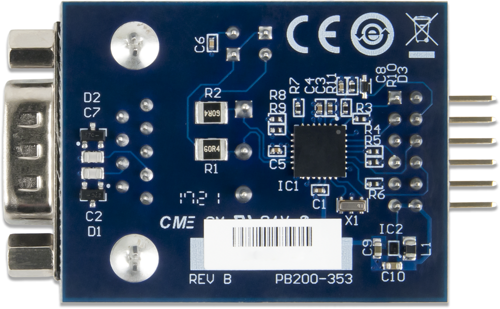
The schematics of the Pmod CAN are available here. Additional information about the CAN controller and transceiver including communication modes and specific timings of the chip can be found in the datasheet here.
Example code demonstrating how to get information from the Pmod CAN can be found on its Resource Center here.
If you have any questions or comments about the Pmod CAN, feel free to post them under the appropriate section (“Add-on Boards”) of the Digilent Forum.