Lab 3: Amplifier Frequency Response
This lab introduces students to the importance of frequency response when designing circuits. Students will investigate the frequency response of two amplifier circuits, one made with transistors and the other using opamps. By comparing how their frequency responses differ while still providing the same overall function, students will learn about how different input frequency ranges affect design considerations. Advanced students can challenge themselves to research high-speed opamps and compare their designs and specifications to regular opamps.
Introduction
Frequency response analysis is used to understand how a circuit behaves at different frequency ranges. In the first two labs, we saw how the frequency response is considered in the design of active and passive filters. In fact, the frequency response of a circuit is not only a big component of just filter circuits but applies to any circuit design. Furthermore, two different circuits that provide the same function may have vastly different frequency responses. In this case, it is important to understand the frequency response of each circuit in order to choose the best design for any given frequency application. In this lab, you will look at two voltage amplifier circuits, the common-emitter (CE) and the inverting operational amplifier (opamp), and investigate their frequency responses.
A voltage amplifier is a circuit that takes an input voltage signal and outputs a larger voltage signal. The CE amplifier you will investigate utilizes an NPN transistor with resistors and capacitors used to set the gain and frequency response. In this lab, you will not learn how to select the resistor or capacitor values for a desired voltage gain, rather, you will learn how the CE amplifier behaves with various frequency ranges and how that is reflected on the frequency response analysis of the circuit.
The opamp is a popular method of voltage amplification; it is much easier to use compared to the CE amplifier and requires fewer components. For this lab, we configured the opamp in an inverting amplifier configuration and we will explore the frequency response of the opamp to see how it relates to different parameters of the opamp IC.
Learning Objectives
In this section, students will:
- Simulate a CE amplifier and opamp open loop gain using Multisim.
- Build a CE amplifier and an inverting opamp amplifier and measure the output gain and frequency response using instruments from WaveForms.
Part List
The following equipment is required for this experiment:
Hardware
- 2N3904, or compatible NPN transistor
- 741, or compatible operational amplifier
- 22μF electrolytic capacitor
- 10μF electrolytic capacitor
- 4.7μF electrolytic capacitor
- 10KΩ resistor
- 5.6KΩ resistor
- 2.2KΩ resistor
- 1.8KΩ resistor
- 2x 1KΩ resistor
- 680Ω resistor
Software
Circuit Theory and Simulation
Common Emitter Amplifier
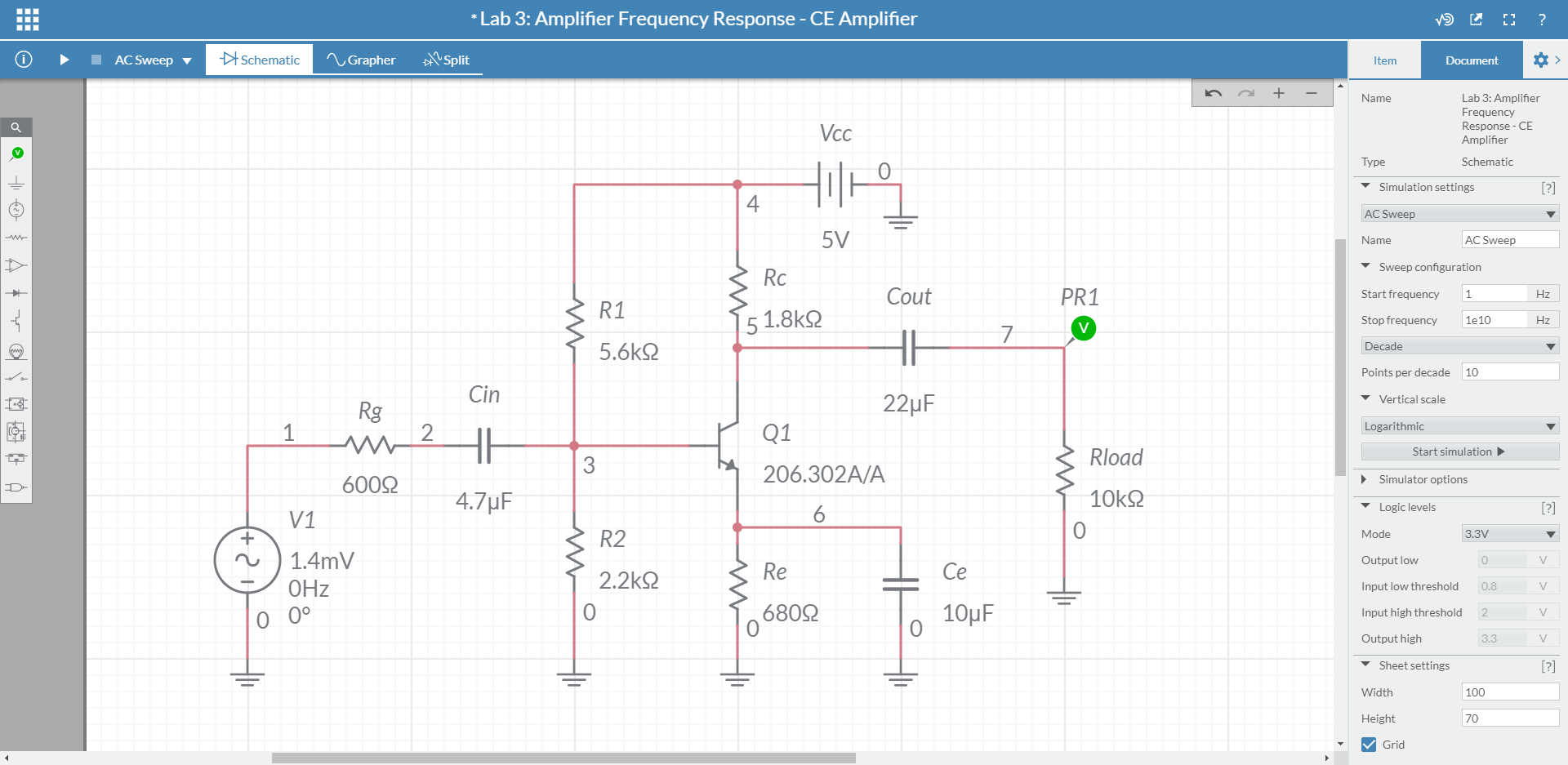
The circuit in the image is a CE amplifier that uses an NPN transistor. In a CE amplifier, the voltage gain is set by choosing the appropriate resistors and capacitors. As mentioned earlier, in this lab we will be more concerned with the frequency response than the design parameters. Table 1 provides DC and AC quantities you can use to analyze the amplifier frequency response.
You can find the model of the 2N3904G NPN transistor in Multisim if you have a premium account. In the free version, you can select the generic NPN transistor model, open Advanced parameters, and complete the fields with the values from the attached document: 2N3904G.zip, leaving the remaining fields on their default value.
| DC Parameters | AC Parameters | ||
|---|---|---|---|
| ${\beta}$ | 135 | Emitter AC resistance ($r_e$) | 25Ω |
| $V_{base}$ | 1.41V | Collector AC resistance ($r_c$) | 1525Ω |
| $V_{emitter}$ | 0.71V | ||
| $V_{collector}$ | 3.12V | ||
| $I_e=I_c$ | 1.00mA | ||
Critical Frequency
The image to the right shows the frequency response of the CE amplifier. There are three sections you want to investigate:
- Low critical frequency ($f_{cl}$) when the gain increases as the frequency increases.
- Mid-range is where the output voltage is maximum. This range is where your amplifier should operate.
- High critical frequency ($f_{ch}$) when the gain decreases as frequency increases.
The goal of this lab is to learn about the low and high critical frequencies. The range between the low and high critical frequencies is the operational bandwidth of your amplifier. Good design dictates that we build in some amount of tolerance into the bandwidth, so we will multiply the low frequency by 10 and divide the high frequency by 10 to calculate the amplifier bandwidth.
Build the circuit using Multisim Live. Set the AC source to 10mV and 30kHz and run the Transient analysis to view the circuit gain in the time domain.
Run the AC sweep analysis to see the circuit's frequency response.
Input Coupling Capacitor
The CE amplifier has three capacitors, to understand how each capacitor affects the frequency response, we will investigate each one individually. The critical frequency can be calculated using the following equation: $f_c=\frac{1}{2{\pi}RC}$.
Thevenin’s Theorem can be used to derive the resistance as seen by the capacitor $C_{in}$. $R_{in}$ is a resistance from $R_1$, $R_2$, and the transistor AC resistance in parallel with each other. You can calculate $R_{in}$ with the following formula: $\frac{1}{R_{in}}=\frac{1}{R_1}+\frac{1}{R_2}+\frac{1}{{\beta}r_e}$.
The total resistance as seen from the source voltage is: $r_{th}=R_{in}+R_g$.
Output Coupling Capacitor
The coupling capacitor $C_{out}$ is affected by the load resistor $R_{load}$ and $R_c$, therefore: $r_{th}=R_c+R_1$.
Emitter Bypass Capacitor
The equivalent resistance seen by the emitter capacitor is given by: $r_{th}=r_e+\frac{R_g||R_1||R_2}{\beta}$.
The resistor $R_e$ is not included in the equation because it is very large when compared to $r_{th}$ in the above equation, recall when two resistors are in parallel, the total resistance is closer to the smaller value.
Once you have calculated the critical frequency for all three capacitors, the overall amplifier low critical frequency $f_{cl}$ is simply the highest frequency you calculated.
High Critical Frequency
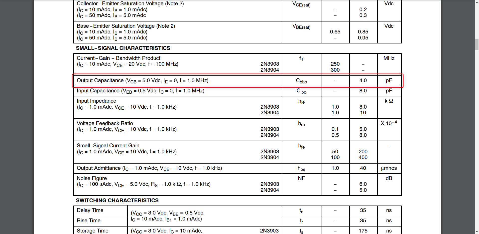
At high frequency, the capacitance that exists inside the transistor begins to affect the circuit output. The 2N3094 On Semiconductor datasheet lists the output capacitance, $C_{obo}$, as 4pF.
Another source of capacitance that will appear in your circuit is parasitic capacitance. This capacitance exists in every component, and in wires, and circuit elements that are close to each other. As the frequency increases, these unwanted capacitances will alter the circuit behavior and causes the output to decrease.
You can approximate the critical high frequency using: $C = C_{obo}+C_{para}$, $r_{th}=R_c||R_1$.
- Questions and Exercises
-
- Calculate the critical frequency for the capacitor $C_{in}$.
- Calculate the critical frequency for the capacitor $C_{out}$.
- Calculate the critical frequency for the emitter capacitor $C_e$.
- Approximate the high critical frequency if $C_{para}=10pF$.
- What highest frequency should you safely use the amplifier?
- What is the maximum gain of the amplifier?
- Multiply the maximum gain by 0.707 to calculate the low critical frequency. Compare your calculation with the simulation result. What can cause the discrepancy between the calculation and simulation?
- Above what frequency should you operate the amplifier?
Opamp Amplifier Frequency Response
The opamp is very popular and has many usages, it requires few external components and is easy to design. The image to the right shows an open-loop amplifier. In this case you can calculate the opamp gain using the following equation: $V_{out}=A_o(V_{in+}-V_{in-})$, where $A_o$ is the open-loop gain.
Build the circuit open-loop amplifier using Multisim Live. Use the 3-terminal opamp model. The 3-terminal opamp model has a default internal ±12V supply. Change the $V_{omp}$ and $V_{omn}$ to ±100V to modify the internal opamp supply to ±100V. The internal supply simulates the voltage range used to power an actual opamp ic. Notice that the opamp gain $A_{vol}$ is 200k.
Set the source frequency to 100Hz, then simulate the circuit. Repeat this step for 1MHz, 10Mhz. As you increase the AC source frequency, what happens to the output voltage?
Run the AC sweep analysis to view the open-loop opamp frequency response.
- Questions and Exercises
-
- As you increase the AC source frequency, what happens to the output voltage?
- Using the response from the grapher, what is the bandwidth of before the opamp begins to roll off?
- How does the opamp internal voltage supply affect the gain?
Gain Bandwidth Product
The open-loop configuration is not used in practice. Usually, there is a feedback connection between the output and one input. An example circuit with feedback is the inverting amplifier.
The gain of the inverting amplifier given by: $A=-\frac{R_2}{R_1}$. When $R_1$ and $R_2$ are 1kΩ, the gain is held constant at 1. You can see that reducing the gain gives your circuit a greater operating bandwidth.
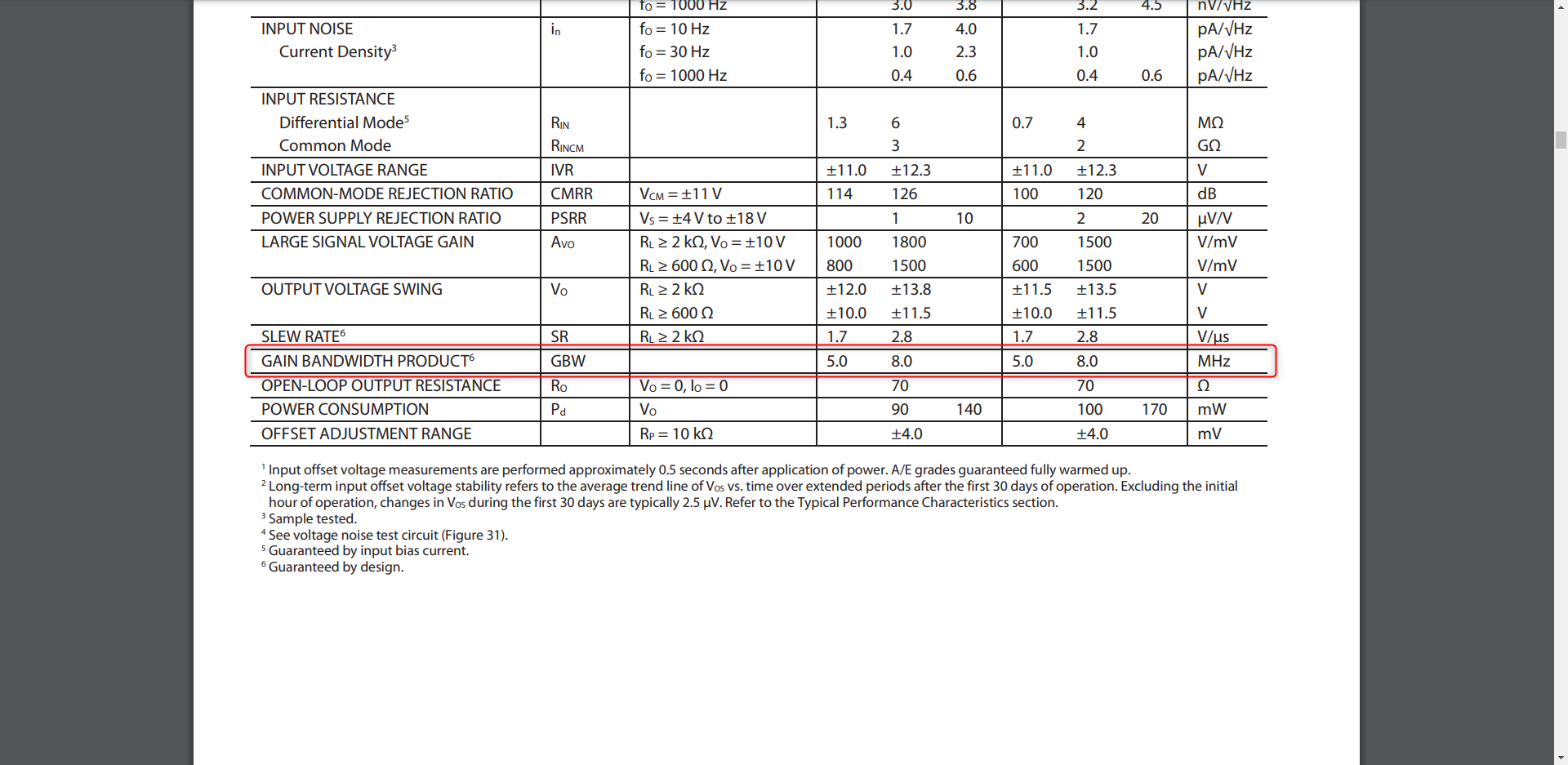
The relationship between gain and bandwidth can be seen in the following equation: $GBW=Af_c$, where $GBW$ is the gain bandwidth product, $A$ is the circuit gains and $f_c$ is the frequency where the output begins to roll off (bandwidth). You can obtain the GBW from the datasheet, here is an example that was taken from the Analog Devices OP27 datasheet.
- Questions and Exercises
-
- Download your opamp datasheet and locate the gain bandwidth product. Design a circuit where the bandwidth is 100kHz. What is maximum gain the circuit can achieve?
Slew Rate
The opamp contains many transistors similar to what we discussed in the CE amplifier section, at high frequencies the capacitors inside the transistor begins to affect the output. In addition to parasitic capacitance, the opamp also has a compensation capacitor. The compensation capacitor is added to give a predictable frequency response and to prevent oscillation.
The first stage inside the opamp is the differential amplifier shown in the image to the right. This circuit compares the input voltage at the opamp input terminals. The compensation capacitor is at the differential output. If you recall, a capacitor has an exponential charging rate which has a certain slope. When the input signal frequency is high, the slope of the input signal is greater than the slope of the compensation capacitor, as a result, the capacitor can cause distortion known as slew rate distortion.
From the Analog Device OP27 datasheet, you can see the slew rate given in V/μs unit. This value tells you the slope of the compensation capacitor.
If the input signal is a sine wave, you can calculate the slope using the following equation: $S_S=2{\pi}fV_p$, where $S_S$ is the slope of the sine wave, $f$ is the signal frequency and $V_p$ is the peak input voltage.
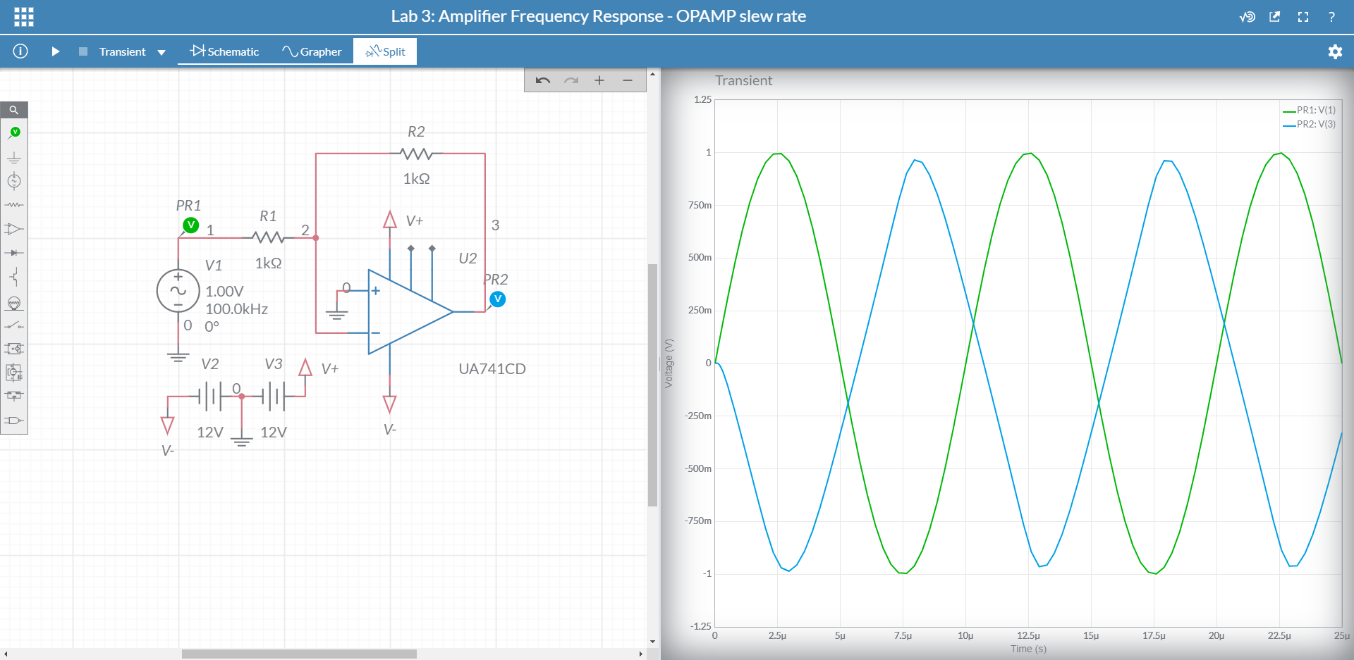
Use Multisim Live to investigate the effect of the slew rate. Build an inverting opamp amplifier and run the transient analysis. Gradually increase the input signal frequency until you can see the effect of slew rate distortion.
To have a more visible slew rate distortion, you can use the UA741CD opamp model. Don't forget to connect the power supplies to this opamp.
- Questions and Exercises
-
- If the input signal is a sine wave, what is the maximum frequency before the display slew rate distortion?
- Locate the frequency response graph for your opamp. What is the bandwidth when the gain is 1?
- Build a buffer with a gain of 1 using an opamp. Compare the frequency response with the datasheet.
Building and Measuring Your Circuit
CE Amplifier
Build the circuit presented in CE Amplifier on the Breadboard Canvas. You can leave out the 600Ω resistor ($R_g$), as it simulates the output impedance of the function generator. You will need to power the circuit with +5V (red wire). Connect the function generator's W1 channel (yellow wire) and the oscilloscope's Channel 1+ (orange wire) to the input of the circuit and the 2+ channel of the oscilloscope (blue wire) to the output of the circuit. Ground the 1- and 2- channels of the oscilloscope (orange-white and blue-white wires), the function generator's ground, and the positive input of the opamp.
Don't forget to turn the Scope Channel 1 and Scope Channel 2 switches towards the MTE headers and the 5V switch towards the POWER label.
You can download the wiring diagram here: wiring_diagram_ce.zip
Launch WaveForms, generate a 50kHz signal using the Wavegen instrument, and set the amplitude to 10mV. Use the Scope to view the circuit response in the time domain.
Open the Network Analyzer and sweep the frequency range from 1 Hz to 10 MHz. Compare the result with the simulation and calculations.
- Questions and Exercises
-
- Compare the measured results with the simulation results. If your response is different than the simulation, explain the reasons for the discrepancies.
- If your application requires a wider bandwidth, what changes would you make to the design?
Investigating the Opamp Frequency Response
Build the circuit presented in Slew Rate on the Breadboard Canvas. You will need to power the opamp with ±12V (red and white wires). Connect the function generator's W1 channel (yellow wire) and the oscilloscope's Channel 1+ (orange wire) to the input of the circuit and the 2+ channel of the oscilloscope (blue wire) to the output of the circuit. Ground the 1- and 2- channels of the oscilloscope (orange-white and blue-white wires), the function generator's ground and the positive input of the opamp.
Don't forget to turn the Scope Channel 1 and Scope Channel 2 switches towards the MTE headers and the 12V± switch towards the POWER label.
You can download the wiring diagram here: wiring_diagram_opamp.zip.
In WaveForms start the Wavegen and the Scope instruments. Set the Wavegen to generate a 1kHz sinusoidal signal and gradually increase the frequency until you see the effect of the slew rate. Use the Scope to view the circuit response in the time domain.
- Questions and Exercises
-
- How does the measured circuit response bandwidth compare with the open-loop gain graph from the datasheet?
- What are some advantages and disadvantages of using the CE amplifier over the opamp?
Further Exploration
High Frequency Components
In this lab, you investigated how frequency affects the limit at which your circuit can operate. You learned about the CE amplifier frequency response. You also learned about the opamp bandwidth and compensation capacitor; you saw how it could cause slew rate distortion when operating at high frequency. These are the reasons why opamps are generally used in low-frequency applications. When designing a circuit that operates at high frequency ranges (MHz), the designer needs to take into consideration internal capacitance and also parasitic capacitance. Often, ICs are specifically made to take into account these considerations. For example, instead of a regular opamp, you can purchase a high-speed opamp. Compare some of the specs of the opamp you used in this lab with the datasheet of a high-speed opamp. Which of the specs discussed in the lab relate to high-speed operation? How do these specs compare between the regular opamp and the high-speed opamp?
Next Steps
For more complementary laboratories, return to the Complementary Labs for Electrical Engineering page of this wiki.
For technical support, please visit the Test and Measurement section of the Digilent Forums.


