JTAG-SMT4 Reference Manual
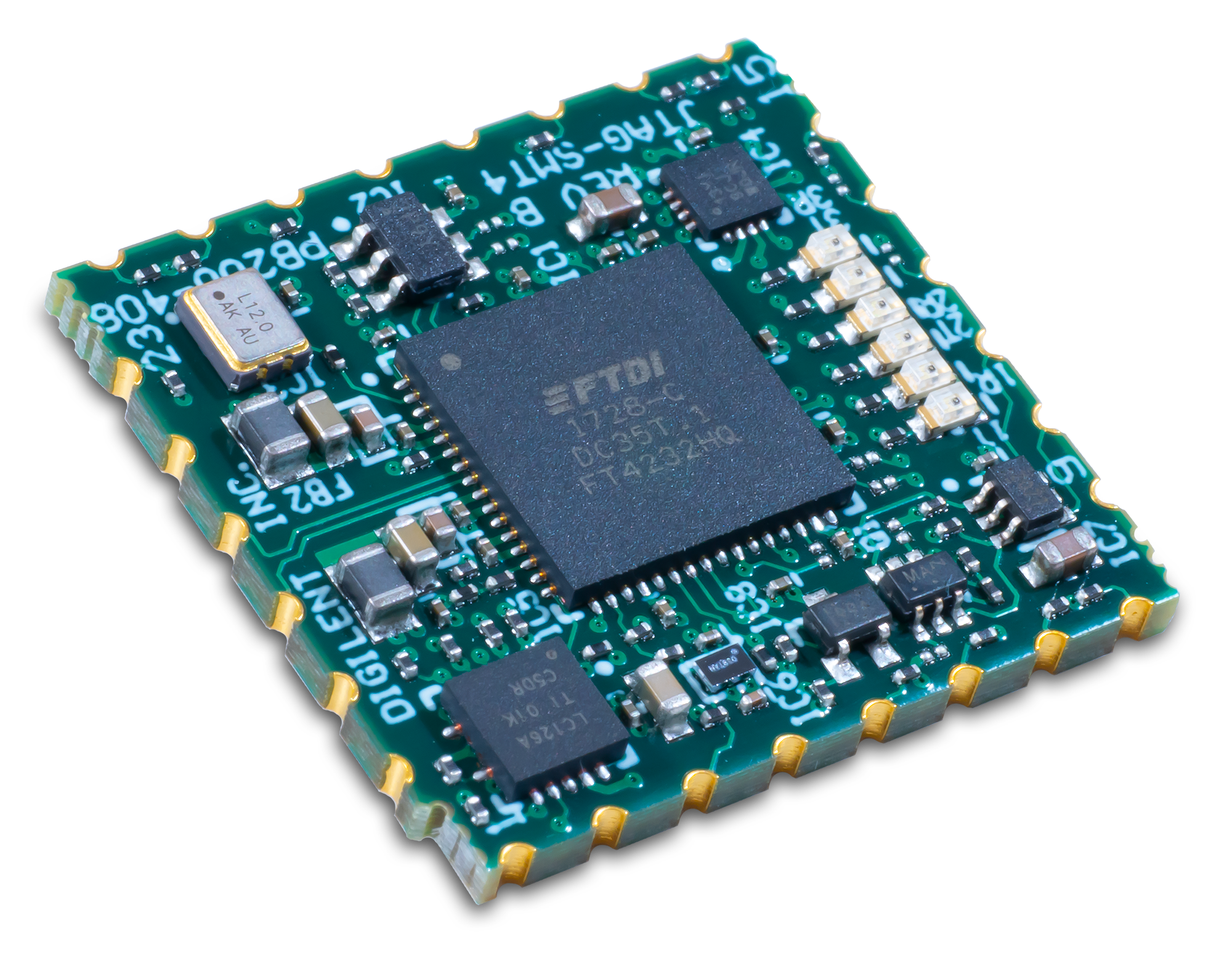
The Joint Test Action Group (JTAG)-SMT4 is a compact, complete, and fully self-contained surface-mount programming module for Xilinx field-programmable gate arrays (FPGAs). The module can be accessed directly from all Xilinx Tools, including Vivado, and Vitis. Users can load the module directly onto a target board and reflow it like any other component.
The JTAG-SMT4 uses a 3.3V main power supply (VDD) and an independent Vref supply to drive the JTAG signals. All JTAG signals use high speed 24mA three-state buffers that allow signal voltages from 1.8V to 3.3V, and bus speeds up to 30MBit/sec. The UART signals are driven directly by the USB controller (referenced to the 3.3V VDD supply) and support bus speeds up to 12Mbaud. The JTAG bus can be shared with other devices as the SMT4 signals are held at high impedance, except when actively driven during programming. The SMT4 module is CE certified and fully compliant with EU RoHS and REACH directives. The module routes the USB D+ (DP) and D- (DM) signals out to pads, providing the system designer with the ability to choose the type of USB connector and its location on the system board.


Features
- Small, complete, all-in-one JTAG programming/debugging solution for Xilinx FPGAs with UART side channel
- Compatible with Xilinx Tools (Vivado/Vitis 2020.1 or newer required)
- Three independent UART channels each supporting bus speeds up to 12Mbaud
- Each UART has transmit and receive LEDs
- High-Speed USB 2.0 port that can drive JTAG bus up to 30Mbit/sec (frequency settable by user)
- Open drain buffers allow PS_SRST_B and PS_POR_B pins to perform software-based resets of Xilinx’s Zynq® platform
- Quad channel USB controller provides simultaneous access to both JTAG and UART interfaces
- Onboard buffers allow JTAG signals to operate at voltages from 1.8V to 3.3V
- Small form-factor surface-mount module can be directly loaded on target boards
- USB D+ and D- signals routed to pads, allowing USB connector to be placed anywhere on the host PCB
- VBUS_DETECT pin allows for reduced current consumption when the module isn’t connected to a PC
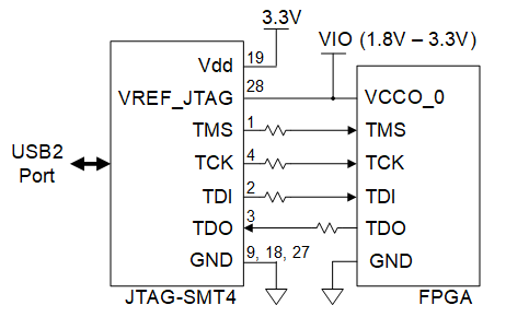
Users can connect JTAG signals directly to the corresponding FPGA signals, as shown in Fig. 1. For best results, mount the module over a ground plane on the host PCB. Although users may run signal traces on top of the host PCB beneath the SMT4, Digilent recommends keeping the area immediately beneath the SMT4 clear.
Note: Keep the impedance between the SMT4 and FPGA below 100 Ohms to operate the JTAG at maximum speed.
Note: If series resistors are used, they should be placed near the transmitting end in order to minimize reflections. Digilent recommends including 0 ohm resistors when space permits, as this will allow the designer to mitigate AC undershoot/overshoot by increasing the series resistance without the need for a PCB spin.
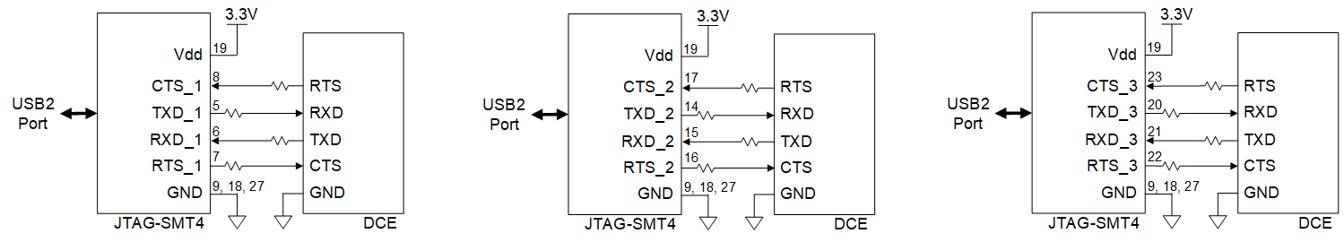
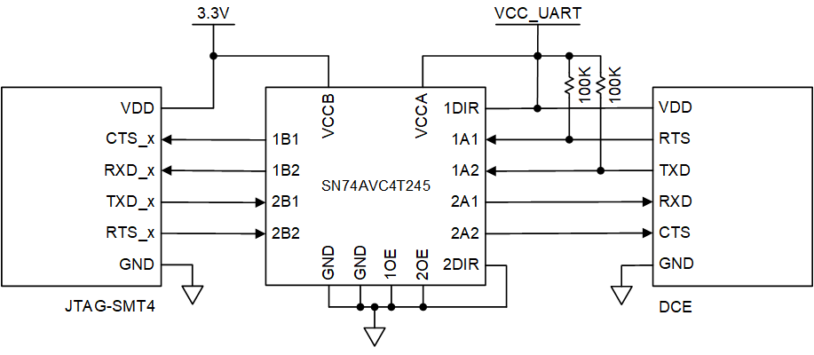
In addition to supporting JTAG, the JTAG-SMT4 also features three UART Interfaces that allow communication with UART peripherals (see Fig. 2). The UART interfaces are presented as virtual com ports on the host PC and support baud rates up to 12Mbaud. The UART interfaces are referenced to VDD and are compatible with 3.3V signaling levels. External level translators may be used to facilitate communication with peripherals operating at different voltage levels (see Fig. 3).

| Callout | Description | Callout | Description |
|---|---|---|---|
| 1 | UART 1 Transmit LED | 4 | UART 2 Receive LED |
| 2 | UART 1 Receive LED | 5 | UART 3 Transmit LED |
| 3 | UART 2 Transmit LED | 6 | UART 3 Receive LED |
Software Support
The JTAG-SMT4 has been designed to work seamlessly with Xilinx’s Vivado and Vitis tool suites. The most recent versions of Vivado and Vitis include all of the drivers, libraries, and plugins necessary to communicate with the JTAG-SMT4. At the time of writing, the following Xilinx software included support for the SMT4: Vivado 2020.1+ and Vitis 2020.1+.
In addition to working seamlessly with Xilinx's Vivado and Vitis tools, Digilent’s Adept software and the Adept software development kit (SDK) support the SMT4 module. For added convenience, customers may freely download the SDK from Digilent’s website. This Adept software includes a full-featured programming environment and a set of public application programming interfaces (API) that allow user applications to directly drive the JTAG chain.
With the Adept SDK, users can create custom applications that will drive JTAG ports on virtually any device. Please see the Adept SDK reference manual for more information.
PS_SRST_B and PS_POR_B Pins
When customers use the JTAG-SMT4 to interface the scan chain of Xilinx’s Zynq platform, they should connect the PS_SRST_B and PS_POR_B pins of the SMT4 to the Zynq’s PS_SRST_B and PS_POR_B pins. These connections allow the Xilinx Tools to reset the Zynq’s processor core at various times during debugging operations. The PS_SRST_B and PS_POR_B pins on the SMT4 are driven by open drain buffers that are capable of sinking up to 32mA of current. Customers who connect these pins must provide external pull-up resistors to the appropriate supply rails. Pull-up resistors between 1K - 100K Ohms are recommended. Please see the following “Application Examples” section for more information.
VBUS_DETECT Pin
The VBUS_DETECT pin is used by the USB controller to determine when VBUS is present. When a logic ‘0’ is detected on this pin, the USB controller is forced into suspend mode. This prevents the SMT4 from forcing current down the USB lines when the host or the hub is powered off. Additionally, it results in reduced current consumption from the module. Connect VBUS directly to the VBUS_DETECT pin as shown in Fig. 5.

Application Examples
Example 1: Interfacing a Zynq-7000
Figure 6 demonstrates how to connect the JTAG-SMT4 to Xilinx’s Zynq-7000 silicon. Please note that VCCO_0, VCCO_MIO0, and VCCO_MIO1 may be powered by the same supply or by different supplies. The PS_SRST_B and PS_POR_B pins of the SMT4 are driven by open drain buffers and therefore an external open drain buffer is not required to add an optional reset button.

Example 2: Interfacing a Zynq-7000 while retaining the Xilinx JTAG Header
Figure 7 below demonstrates how to connect the JTAG-SMT4 to Xilinx’s Zynq-7000 silicon alongside Xilinx’s 14-pin JTAG header. In this example, an open drain buffer allows both the SMT4 and Xilinx JTAG Header to drive the PS_SRST_B pin, which may operate a different voltage than the Zynq’s JTAG pins.

Supported Target Devices
The JTAG-SMT4 is capable of targeting the following Xilinx devices:
- Xilinx FPGAs, including UltraScale+
- Xilinx SoCs, MPSoCs, and RFSoCs, including Xilinx Zynq-7000 and Zynq UltraScale+
- Xilinx ACAPs, including Versal
- Xilinx CoolRunner™/CoolRunner-II CPLDs
- Xilinx Platform Flash ISP configuration PROMs1)
- Select third-party SPI PROMs2)
- Select third-party BPI PROMs3)
The following devices cannot be targeted by the JTAG-SMT4:
- Xilinx 9500/9500XL CPLDs
- Xilinx 1700 and 18V00 ISP configuration PROMs
- Xilinx FPGA eFUSE programming
Programming Solutions Comparison Chart
| JTAG-SMT4 | JTAG-SMT3-NC | JTAG-SMT2 | JTAG-SMT2-NC | |
|---|---|---|---|---|
| Max Speed | 30 MHz | 30 MHz | 30 MHz | 30 MHz |
| Voltage Range | 1.8V - 3.3V | 1.8V – 5V | 1.8V – 5V | 1.8V – 5V |
| Xilinx Native Support | Vivado / Vitis 2020.1+ | ISE 14.1+ Vivado 2014.1 | ISE 14.1+ Vivado 2013.1+ | ISE 14.1+ Vivado 2013.1+ |
| Xilinx Plug-in Support | NONE | ISE 13.1+ | ISE 13.1+ | ISE 13.1+ |
| Digilent Adept Support | YES | YES | YES | YES |
| PC Interface | USB | USB | USB | USB |
| Onboard USB Connector | YES | YES | YES | NO |
| Host Board Connector Interface | 28-pad SMT | 18-pad SMT | 11-pad SMT | 13-pad SMT |
| 4-Wire JTAG | YES | YES | YES | YES |
| 2-Wire JTAG | NO | NO | YES | YES |
| Zynq PS_SRST_B Support | YES | YES | YES | YES |
| Zynq PS_POR_B Support | YES | NO | NO | NO |
| SPI Support | NO | NO | YES | YES |
| Independent UART Channels | 3 | 1 | 0 | 0 |
Pinout Table
| Pin Number | Pin Name | Pin Number | Pin Name |
|---|---|---|---|
| 1 | TMS | 15 | RXD_2 |
| 2 | TDI | 16 | RTS_2 |
| 3 | TDO | 17 | CTS_2 |
| 4 | TCK | 18 | GND |
| 5 | TXD_1 | 19 | VDD |
| 6 | RXD_1 | 20 | TXD_3 |
| 7 | RTS_1 | 21 | RXD_3 |
| 8 | CTS_1 | 22 | RTS_3 |
| 9 | GND | 23 | CTS_3 |
| 10 | PS_POR_B | 24 | VBUS_DETECT |
| 11 | PS_SRST_B | 25 | USB D- |
| 12 | NC | 26 | USB D+ |
| 13 | NC | 27 | GND |
| 14 | TXD_2 | 28 | VREF_JTAG |
Mechanical Information


General USB Signal Routing Guidelines
- Maintain a differential impedance of 90 Ohms between the DP and DM signals.
- Keep DP and DM trace lengths within 50 mils of each other.
- Minimize DP and DM signal trace length. Keeping the trace length below 3 inches is recommended.
- When possible, route DP and DM on the plane closest to the ground plane.
- When possible, avoid routing the DP and DM signals through vias. If vias cannot be avoided, then keep them small and place the DP and DM traces on the same layer.
- When possible, avoid routing other traces near DP and DM.
- When possible, minimize or avoid the use of bends in the DP and DM traces. If 90 degree bends are necessary, then use two 45 degree turns or an arc instead of a single 90 degree turn.
- Do NOT route DP or DM near oscillators, crystals, switching regulators, clock generators, or inductors.
Absolute Maximum Ratings
| Symbol | Parameter | Condition | Min | Max | Unit |
|---|---|---|---|---|---|
| Vdd | Operating supply voltage | -0.3 | 4.0 | V | |
| Vref | I/O reference/supply voltage | -0.5 | 6.5 | V | |
| VIO | JTAG Signal Voltage | -0.5 | 6.5 | V | |
| UART Signal Voltage | -0.3 | Vdd + 0.5 | V | ||
| IIK,IOK | TMS, TCK, TDI, TDO, PS_SRST_B, PS_POR_B DC Input/Output Diode Current | VIO < -0.3V | -50 | mA | |
| VIO > 6V | +20 | ||||
| IOUT | JTAG DC Output Current | ±50 | mA | ||
| UART DC Output Current | ±16 | mA | |||
| TSTG | Storage Temperature | -10 | +60 | ºC | |
| ESD | Human Body Model JEDEC EIA/JESD22-A114-B, Class 2 | 2000 | V | ||
| Charge Device Model JEDEC EIA/JESD22-C101-D, Class-III | 500 | V | |||
DC Operating Characteristics
| Symbol | Parameter | Min | Typ | Max | Unit |
|---|---|---|---|---|---|
| Vdd | Operating supply voltage | 3.0 | 3.3 | 3.6 | Volts |
| VREF_JTAG | JTAG I/O reference/supply voltage | 1.65 | 3.3 | 3.6 | Volts |
| TDO | Input High Voltage (VIH) | 0.65 x VREF_JTAG | 5.5 | Volts | |
| Input Low Voltage (VIL) | 0 | 0.55 | Volts | ||
| RXD_1, RXD_2, RX_3, CTS_1, CTS_2, CTS_3 | Input High Voltage (VIH) | 2.0 | Vdd | Volts | |
| Input Low Voltage (VIL) | 0 | 0.8 | Volts | ||
| VBUS_DETECT | Input High Voltage (VIH) | 3.1 | 5.7 | Volts | |
| Input Low Voltage (VIL) | 0 | 0.8 | Volts | ||
| TMS, TCK, TDI | Output High (VOH) | 0.725 x Vref | 0.95 x Vref | Vref | Volts |
| Output Low (VOL) | 0 | 0.05 x Vref | 0.8 | Volts | |
| TXD_1, TXD_2, TXD_3, RTS_1, RTS_2, RTS_3 | Output High (VOH) | 2.4 | Vdd | Volts | |
| Output Low (VOL) | 0 | 0.4 | Volts | ||
| PS_SRST_B, PS_POR_B | Output Low (VOL) | 0 | 0.55 | Volts | |
| TA | Operating Temperature | -40 | 85 | ºC |
AC Operating Characteristics
The JTAG-SMT4’s JTAG signals operate according to the timing diagram in Fig. 10. The SMT4 supports JTAG/TCK frequencies from 30 MHz to 8 KHz at integer divisions of 30 MHz from 1 to 3750. Common frequencies include 30 MHz, 15 MHz, 10 Mhz, 7.5 MHz, and 6 MHz. The JTAG/TCK operating frequency can be set within the Xilinx tools.

| Symbol | Parameter | Min | Max |
|---|---|---|---|
| TCK | TCK period | 30 ns | 125 us |
| TCKH, TCKL | TCLK pulse width | 15 ns | 62.5 us |
| TCD_TMS | TCLK to TMS | 1 ns | 8.15 ns |
| TCD_TDI | TCLK to TDI | 1 ns | 8.15 ns |
| TSETUP | TDO Setup Time | 15.7 ns | |
| THD | TDO Hold Time | 0 ns |
Mounting to Host PCBs
The JTAG-SMT4 module has a moisture sensitivity level (MSL) of 6. Prior to reflow, the JTAG-SMT4 module must be dried by baking it at 70° C for 72 hours (the tray and the module itself can be baked 125° C for 24 hours, but any labels and rubber feet present on the module cannot withstand this higher temperature). Once this process has been completed, the module has a MSL of 3 and is suitable for reflow for up to 168 hours without additional drying.
The factory finishes the JTAG-SMT4 signal pads with the ENIG process using 2u” gold over 150u” electroless nickel. This makes the SMT4 compatible with most mounting and reflow processes (see Fig. 11). The binding force of the solder is sufficient to hold the SMT4 firmly in place, so mounting should require no additional adhesives.

Packaging
Digilent ships quantities under 40pcs individually packaged in antistatic bags with MSL 6. Digilent will pack and ship larger quantities in groups of 40 positioned in an antistatic bake tray with MSL 3(see Fig. 12). Trays will be packaged in an anti-static vacuum sealed bag. We also offer to bake them before shipping for an additional cost per 40pc lot.
