Using I/O on Digilent FPGA/SoC Boards With LabVIEW LINX Toolkit
Introduction
This guide will walk you through the process of deploying LabVIEW code to Digilent embedded targets for interacting with device peripherals and I/O, including digital, analog, SPI, I2C and UART. The following Digilent boards can be used with this guide:
- Arty Z7-10
- Arty Z7-20
- Cora Z7-07S
- Cora Z7-10
The LabVIEW LINX Toolkit adds support for Arduino, Raspberry Pi and BeagleBone embedded platforms. The Raspberry Pi provider is used to interact with the Digilent boards listed above.
Prerequisites
Hardware
- Arty Z7-10 / Arty Z7-20 / Cora Z7-07S / Cora Z7-10 board
- Micro USB Cable
- for UART communication
- SD card with a minimum capacity of 1GB storage
- Ethernet cord
Software
- Image file: linx-debian-jessie-armhf-rfs.img.zip
- LabVIEW VI Demo Files for each board: Digilent_Demo_LabVIEW_VI_files.zip
- Software to create a bootable microSD card (Win32 Disk Imager is used in this guide)
- Serial Terminal Application (Tera-Term is used in this guide)
Creating The Bootable MicroSD Card
- Start Win32DiskImager and open linx-debian-jessie-armhf-rfs.img.
- Select the drive letter of your microSD.
- Click Write.
On the microSD card, copy into the root directory the files BOOT.BIN and image.ub from the folder of the board you are using.
Eject the microSD card and insert it into the slot on the board.
Connect the Ethernet cable between your board and the router. Attach the microUSB cable between your PC and the board.
Open Tera Term and connect to the serial port of the board with 115200 baud rate, 8 bits, no parity, 1 stop bit.
On the first boot, the root partition on the SD card will automatically resize to make full use of its capacity. A reboot will follow.
Setup The Environment
Log in with the following:
Username: linx
Password: linx
Library setup
Out of the box, the environment is configured for the Arty Z7-20. If you are using one of the other boards, run the following commands:
cd /srv/chroot/labview/usr/lib/
sudo ln -s --force <BOARD SO FILE> liblinxdevice.so
Where <BOARD SO FILE> is:
- liblinxdevice_az710.so for Arty Z7-10
- liblinxdevice_cz707s.so for Cora Z7-07S
- liblinxdevice_cz710.so for Cora Z7-10
Verify the symbolic link is set correctly:
ls-l liblinxdevice.so
If you pointed the symbolic link to a different library, restart the LabVIEW service:
sudo systemctl restart labview.service
Find out the IP address using the command:
ip a
Running The LabVIEW Demo
Unzip digilent_demo_labview_vi_files.zip.
Open NI LabVIEW 2020 and Create Project → Blank Project.
Right-click on project name → New → Targets and Devices.
A Raspberry Pi 2 B target will be added to your project. You can add as many targets as you want to the project.
NOTE: In this guide, the existent Raspberry Pi provider is used to interact with the Digilent boards listed above.
Right-click on Raspberry Pi 2 B → Properties and change the name and the IP address according to the board you are using.
Go to Conditional Disable Symbols and change the LINX DEVICE FAMILY and LINX DEVICE ID.
- LINX DEVICE FAMILY=7 LINX DEVICE ID=11 for Arty Z7-10
- LINX DEVICE FAMILY=7 LINX DEVICE ID=20 for Arty Z7-20
- LINX DEVICE FAMILY=7 LINX DEVICE ID=7 for Cora Z7-07S
- LINX DEVICE FAMILY=7 LINX DEVICE ID=10 for Cora Z7-10
Right-click on target name → Add → File and select the Demo_<name-of-Digilent-board_>.vi from the location you extracted the Digilent_Demo_LabVIEW_VI_files.zip.
Open Demo_<name-of-Digilent-board_>.vi and click the RUN button. Wait for the deployment to complete.
You can access the board I/O from the interface.
NOTE: In this demo:
- IO0-13, IO26-I042, JB1-JB10, JA1-JA9 and LD0-LD3 are output channels (DO Channels)
- SW0-SW1 and BTN0-BTN3 are input channels (DI Channels)
- There is one channel for SPI, one for I2C and one for UART (Channel 0).
- The demo is configured to read over SPI or I2C protocol and to read/write over UART protocol.
- The SPI is configured to read one byte by sending a multibyte structure (3 bytes) wherein the first byte is a command, the second byte is the SPI Register Address and the third byte is 0x00. The user must adapt the block diagram of the Demo_<name-of-Digilent-board_>.vi for the SPI device that is using.
- The A6-A7 differential channel is a unipolar channel and A8-A9, A10-A11 and V_P – V_N are bipolar channels. Please read the XADC User Guide (UG480), Page 31 for more information.
Digilent Boards Pinout
Below you can find the pinout for each board to use it with LabVIEW 2020. This pinout was created to use it specifically with LabVIEW LINX Toolkit and is only compatible with LabVIEW libraries which can be found inside /srv/chroot/labview/usr/lib:
- liblinxdevice_az710.so for Arty Z7-10
- liblinxdevice_az720.so for Arty Z7-20
- liblinxdevice_cz707s.so for Cora Z7-07S
- liblinxdevice_cz710.so for Cora Z7-10
- Arty Z7-10 Pinout
-
NOTE: The Arty Z7-10 board is compatible only with the liblinxdevice_az710.so library.
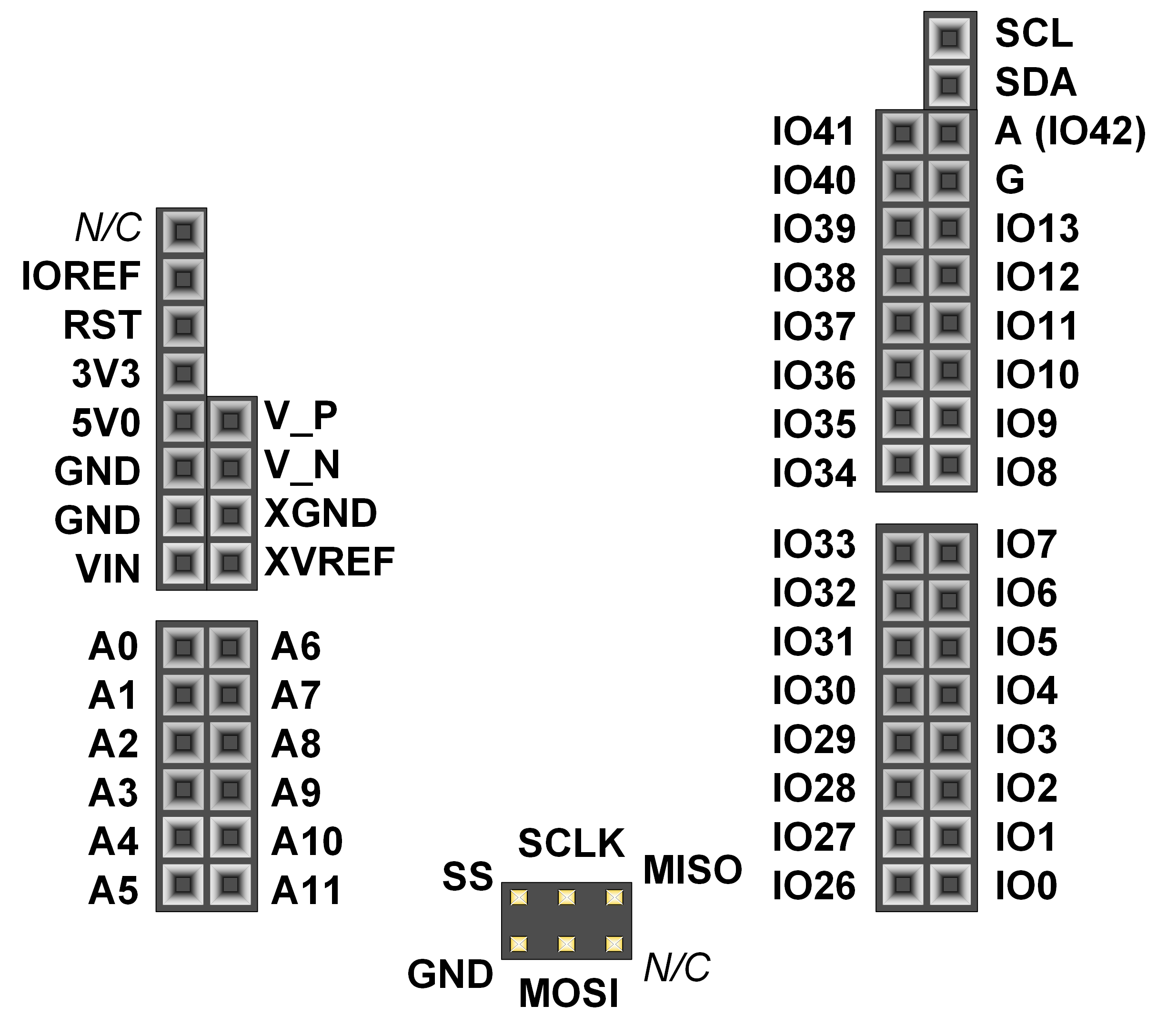
- Shield Connector Pinout
NOTE: IO26-IO41 and A (IO42) are not accessible on the Arty Z7-10.
Channel / Pin Number Pin Name Function Digital Input/Output channels 0 IO0 Arty Z7-10 General purpose I/O pins 1 IO1 2 IO2 3 IO3 4 IO4 5 IO5 6 IO6 7 IO7 8 IO8 9 IO9 10 IO10 11 IO11 12 IO12 13 IO13 Channel 0 SCL I2C Clock SDA I2C Data Channel 0 SCLK SPI Clock. SPI Supported Speeds [Hz]: 7629, 15200, 30500, 61000, 100000. MOSI SPI Data out MISO SPI Data in 38 SS SPI Slave Select Analog Input channels 0 A0 Single-Ended Analog Unipolar Inputs (range of 0V-3.3V). Arty Z7 uses an external circuit to scale down the input voltage from 0V-3.3V to an input range of 0V to 1V. (see UG480 - Unipolar Input Signals) 1 A1 2 A2 3 A3 4 A4 5 A5 67 A6p-A7n UNIPOLAR Differential Analog Inputs (see UG480 - Bipolar Input Signals) 89 A8p-A9n BIPOLAR 111 A10p-A11n BIPOLAR 101 V_P-V_N BIPOLAR - Pmod Connectors Pinout
 Figure 2. Pmod JA Pin Diagram.
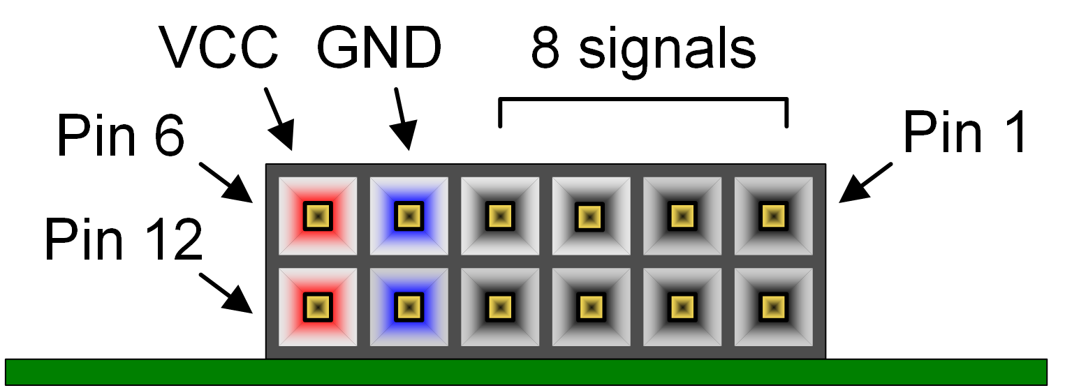 Figure 3. Pmod JB Pin Diagram.
Channel / Pin Number Pin Name Function 24 JA1 Pmod JA General purpose I/O pins 25 JA2 26 JA3 27 JA7 28 JA8 29 JA9 Channel 0 JA4 UART RX UART Supported Baud Rates [bit/s]: 0, 50, 75, 110, 134, 150, 200, 300, 600, 1200, 1800, 2400, 4800, 9600, 19200, 38400, 57600, 115200. JA10 UART TX 30 JB1 Pmod JB General purpose I/O pins 31 JB2 32 JB3 33 JB4 34 JB7 35 JB8 36 JB9 37 JB10 - Push-Buttons Pinout
Push-Button Pin Number Pin Name 20 BTN0 21 BTN1 22 BTN2 23 BTN3 - LEDs Pinout
LED Pin Number Pin Name 16 LED0 17 LED1 18 LED2 19 LED3 - Slide Switches Pinout
Slide Switch Pin Number Pin Name 14 SW0 15 SW1 - RGB LEDs Pinout
File Function /dev/led0 RGB LED LD4. Write to /dev/led0 a hexadecimal number: 0xRRGGBB /dev/led1 RGB LED LD5. Write to /dev/led1 a hexadecimal number: 0xRRGGBB
- Arty Z7-20 Pinout
-
NOTE: The Arty Z7-20 board is compatible only with the liblinxdevice_az720.so library.
- Shield Connector Pinout
Channel / Pin Number Pin Name Function Digital Input/Output channels 0 IO0 Arty Z7-20 General purpose I/O pins 1 IO1 2 IO2 3 IO3 4 IO4 5 IO5 6 IO6 7 IO7 8 IO8 9 IO9 10 IO10 11 IO11 12 IO12 13 IO13 26 IO26 27 IO27 28 IO28 29 IO29 30 IO30 31 IO31 32 IO32 33 IO33 34 IO34 35 IO35 36 IO36 37 IO37 38 IO38 39 IO39 40 IO40 41 IO41 25 A (IO42) Channel 0 SCL I2C Clock SDA I2C Data Channel 0 SCLK SPI Clock. SPI Supported Speeds [Hz]: 7629, 15200, 30500, 61000, 100000. MOSI SPI Data out MISO SPI Data in 24 SS SPI Slave Select Analog Input channels 0 A0 Single-Ended Analog Unipolar Inputs (range of 0V-3.3V). Arty Z7 uses an external circuit to scale down the input voltage from 0V-3.3V to an input range of 0V to 1V. (see UG480 - Unipolar Input Signals) 1 A1 2 A2 3 A3 4 A4 5 A5 67 A6p-A7n UNIPOLAR Differential Analog Inputs (see UG480 - Bipolar Input Signals) 89 A8p-A9n BIPOLAR 111 A10p-A11n BIPOLAR 101 V_P-V_N BIPOLAR - Pmod Connectors Pinout
 Figure 2. Pmod JA Pin Diagram.
 Figure 3. Pmod JB Pin Diagram.
Channel / Pin Number Pin Name Function 42 JA1 Pmod JA General purpose I/O pins 43 JA2 44 JA3 45 JA7 46 JA8 47 JA9 Channel 0 JA4 UART RX UART Supported Baud Rates [bit/s]: 0, 50, 75, 110, 134, 150, 200, 300, 600, 1200, 1800, 2400, 4800, 9600, 19200, 38400, 57600, 115200. JA10 UART TX 48 JB1 Pmod JB General purpose I/O pins 49 JB2 50 JB3 51 JB4 52 JB7 53 JB8 54 JB9 55 JB10 - Push-Buttons Pinout
Push-Button Pin Number Pin Name 14 BTN0 15 BTN1 16 BTN2 17 BTN3 - LEDs Pinout
LED Pin Number Pin Name 18 LED0 19 LED1 20 LED2 21 LED3 - Slide Switches Pinout
Slide Switch Pin Number Pin Name 22 SW0 23 SW1 - RGB LEDs Pinout
File Function /dev/led0 RGB LED LD4. Write to /dev/led0 a hexadecimal number: 0xRRGGBB /dev/led1 RGB LED LD5. Write to /dev/led1 a hexadecimal number: 0xRRGGBB
- Cora Z7-10 and Cora Z7-07S Pinout
-
The Cora Z7-07S board pinout is the same as the Cora Z7-10 board pinout. The only difference between Cora Z7-10 and Cora Z7-07S is the capability of the Zynq part.
NOTE: The Cora Z7-10 board is compatible only with the liblinxdevice_cz710.so library.
NOTE: The Cora Z7-07S board is compatible only with the liblinxdevice_cz707s.so library.
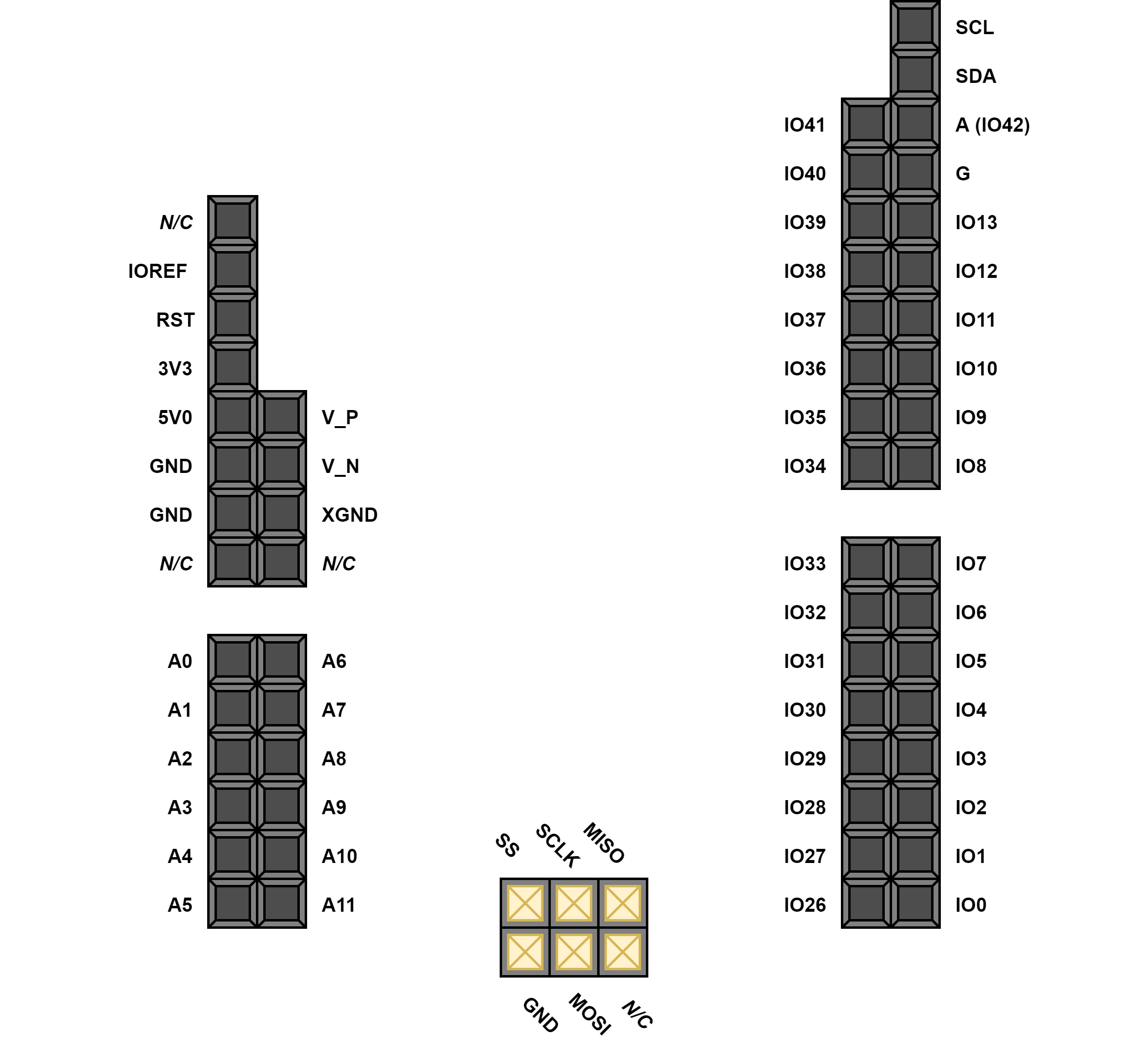
- Shield Connector Pinout
Channel / Pin Number Pin Name Function Digital Input/Output channels 0 IO0 Cora Z7 General purpose I/O pins 1 IO1 2 IO2 3 IO3 4 IO4 5 IO5 6 IO6 7 IO7 8 IO8 9 IO9 10 IO10 11 IO11 12 IO12 13 IO13 26 IO26 27 IO27 28 IO28 29 IO29 30 IO30 31 IO31 32 IO32 33 IO33 34 IO34 35 IO35 36 IO36 37 IO37 38 IO38 39 IO39 40 IO40 41 IO41 25 A (IO42) Channel 0 SCL I2C Clock SDA I2C Data Channel 0 SCLK SPI Clock. SPI Supported Speeds [Hz]: 7629, 15200, 30500, 61000, 100000. MOSI SPI Data out MISO SPI Data in 24 SS SPI Slave Select Analog Input channels 0 A0 Single-Ended Analog Unipolar Inputs (range of 0V-3.3V). Cora Z7 uses an external circuit to scale down the input voltage from 0V-3.3V to an input range of 0V to 1V. (see UG480 - Unipolar Input Signals) 1 A1 2 A2 3 A3 4 A4 5 A5 67 A6p-A7n UNIPOLAR Differential Analog Inputs (see UG480 - Bipolar Input Signals) 89 A8p-A9n BIPOLAR 111 A10p-A11n BIPOLAR 101 V_P-V_N BIPOLAR - Unloaded Expansion Header Pinout
 Figure 2. Unloaded Expansion Header Pin Diagram.
Pin Number Pin Name Function 48 IO2 Unloaded Expansion Header General purpose I/O pins 49 IO3 50 IO4 51 IO5 52 IO6 53 IO7 54 IO8 55 IO9 56 IO10 57 IO11 58 IO12 59 IO13 - Pmod Connectors Pinout
 Figure 2. Pmod JA Pin Diagram.
 Figure 3. Pmod JB Pin Diagram.
Channel / Pin Number Pin Name Function 42 JA1 Pmod JA General purpose I/O pins 43 JA2 44 JA3 45 JA7 46 JA8 47 JA9 Channel 0 JA4 UART RX UART Supported Baud Rates [bit/s]: 0, 50, 75, 110, 134, 150, 200, 300, 600, 1200, 1800, 2400, 4800, 9600, 19200, 38400, 57600, 115200. JA10 UART TX 16 JB1 Pmod JB General purpose I/O pins 17 JB2 18 JB3 19 JB4 20 JB7 21 JB8 22 JB9 23 JB10 - Push-Buttons Pinout
Push-Button Pin Number Pin Name 14 BTN0 15 BTN1 - RGB LEDs Pinout
File Function /dev/led0 RGB LED LD0. Write to /dev/led0 a hexadecimal number: 0xRRGGBB /dev/led1 RGB LED LD1. Write to /dev/led1 a hexadecimal number: 0xRRGGBB


