Cmod A7 Reference Manual
The Cmod A7-15T variant is now retired and no longer for sale in our store. The Cmod A7-35T is still available.
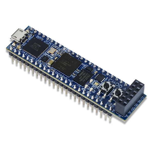
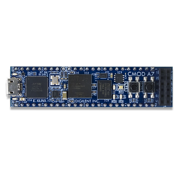
The Digilent Cmod A7 is a small, 48-pin DIP form factor board built around a Xilinx Artix 7 FPGA. The board also includes a USB-JTAG programming circuit, USB-UART bridge, clock source, Pmod host connector, SRAM, Quad SPI Flash, and basic I/O devices. These components make it a formidable, albeit compact, platform for digital logic circuits and Microblaze embedded softcore processor designs alike. There are 44 Digital FPGA I/O signals and 2 FPGA Analog inputs that are routed to 100-mil-spaced through-hole pins so that you can integrate your programmable logic design directly into a solderless breadboard circuit. At just .7” by 2.75” inches, it can also be loaded in a standard socket and used in embedded systems.

Download This Reference Manual
Features
- System Features
- 512KB SRAM with an 8-bit bus and 8ns access times
- 4MB Quad-SPI Flash
- USB-JTAG Programming Circuitry
- Powered from USB or external 3.3-5.5V supply connected to DIP pins
- System Connectivity
- USB-UART bridge
- Interaction and Sensory Devices
- 2 LEDs
- 1 RGB LED
- 2 Push Buttons
- Expansion Connectors
- 48-pin DIP connector with 44 Digital I/O and 2 Analog inputs (0-3.3V)
- One Pmod connector with 8 Digital I/O
The Cmod A7 can be purchased with either an Artix-15T or Artix-35T FPGA. These two Cmod A7 product variants are referred to as the Cmod A7-15T and Cmod A7-35T, respectively. When Digilent documentation describes functionality that is common to both of these variants, they are referred to collectively as the “Cmod A7”. When describing something that is only common to a specific variant, the variant will be explicitly called out by its name.
The only difference between the Cmod A7-15T and Cmod A7-35T are the capabilities of the FPGA found on the board. They compare as follows:
| Product Variant | Cmod A7-35T | Cmod A7-15T (No longer in production) |
|---|---|---|
| FPGA Part | XC7A35T-1CPG236C | XC7A15T-1CPG236C |
| 1 MSPS On-chip ADC | Yes | Yes |
| Programming options | Quad-SPI Flash/JTAG | Quad-SPI Flash/JTAG |
| Look-up Tables (LUTs) | 20,800 | 10,400 |
| Flip-Flops | 41,600 | 20,800 |
| Block RAM | 225 KB | 112.5 KB |
| Clock Management Tiles | 5 | 5 |
The Cmod A7 is fully compatible with the high-performance Vivado ® Design Suite. It is supported under the free WebPACK™ license, so designs can be implemented at no additional cost. This free license includes the ability to create MicroBlaze™ soft-core processor designs. Design resources, example projects, and tutorials are available for download at the Cmod A7 Resource Center, accessible from Digilent Reference.
1 Power Supplies
The Cmod A7 uses a Linear Technologies LTC3569 triple output buck power regulator to generate the needed voltages for the onboard components. It is connected as shown in Figure 1.1. The characteristics of the outputs are shown in Table 1.1.

Figure 1.1. Cmod A7 Power Supply.
| Net name | Upstream net name | Power IC Type | Power IC Label | Min/Typ/Max Voltage | Max. Current | Major Devices and Connectors |
|---|---|---|---|---|---|---|
| VCC1V0 | VU | Switching PS | IC10 | 0.95V/1.00V/1.05V | 1.2A | FPGA Core and Block RAM |
| VCC1V8 | VU | Switching PS | IC10 | 1.71V/1.80V/1.89V | 0.6A | FPGA AUX and ADC, USB Core |
| VCC3V3 | VU | Switching PS | IC10 | 3.135V/3.30V/3.465V | 0.6A | SRAM, USB Controller, PMOD, LEDS, Buttons, FPGA USER I/O |
Table 1.1. Power Rail Characteristics.
1.1 Power Input Options
It is possible to power the Cmod A7 from either USB or from an external power supply attached to pins 24 and 25 of the DIP connector, labeled “VU” and GND“ respectively. The required characteristics of a power source attached to either of these two options is outlined in Table 1.1.1.
| Connector Type | Connector Label | Schematic net name | Min/Rec/Max Voltage |
|---|---|---|---|
| USB | J3 | USB5V0 | 4.5/5/5.5 |
| DIP | J1 (Pin 24) | VU | 3.32/5/5.5 |
The minimum external voltage that can be applied to VU depends on the amount of current drawn from the VCC3V3 rail via the Pmod header. With 0mA drawn from the Pmod header the minimum external voltage is 3.32V. With 100mA drawn from the Pmod header the minimum external voltage is 3.38V. With 250mA drawn from the Pmod header the minimum external voltage is 3.48V.
When the Cmod A7 is being powered by the USB connector, the voltage from the USB device is driven onto the VU pin. This allows you to power an external circuit from the USB host in addition to the Cmod A7. The VU pin is driven via a schottky diode, so a small voltage drop will occur, but it should be assumed the voltage present on VU will be close to 5V.
It is possible to power the Cmod A7 through both the USB connector and external power through the VU pin. However, a schottky diode will be required to be added in series with the VU pin. More details can be found on this Digilent Forum thread here.
Warning: When a USB host is attached to the micro USB connector, the VU pin on the DIP connector (pin 24) is driven to the voltage being provided by the USB host (typically between 4.5V-5.5V). If you have a power source attached to the VU pin, you must disconnect it before attaching a USB host, or risk damaging it. This can be particularly dangerous if the power source is a battery.
2 FPGA Configuration
After power-on, the Artix-7 FPGA must be configured (or programmed) before it can perform any functions. You can configure the FPGA in one of two ways:
- A PC can use the Digilent USB-JTAG circuitry to program the FPGA any time the power is on.
- A file stored in the nonvolatile serial (Quad-SPI) flash device can be transferred to the FPGA using the SPI port.
On power-up the Cmod A7 is programmed by the Quad-SPI flash. If the FPGA does not find a valid configuration file in the flash, then it will remain unconfigured until it is programmed over JTAG.
The FPGA configuration data is stored in files called bitstreams that have the .bit file extension. The Vivado software from Xilinx can create bitstreams from VHDL or Verilog® based source files.
Bitstreams are stored in volatile memory cells within the FPGA. This data defines the FPGA’s logic functions and circuit connections, and it remains valid until it is erased by removing board power or by writing a new configuration file using the JTAG port.
Both the Artix-7 35T and 15T bitstreams are typically 17,536,096 bits. The time it takes to program the Cmod A7 can be decreased by compressing the bitstream before programming, and then allowing the FPGA to decompress the bitstream itself during configuration. Depending on design complexity, compression ratios of 10x can be achieved. Bitstream compression can be enabled within the Vivado tools to occur during generation. For instructions on how to do this, consult the Xilinx documentation for Vivado.
After being successfully programmed, the FPGA will cause the “DONE” LED to illuminate.
The following sections provide greater detail about programming the Cmod A7 using the different methods available.
2.1 JTAG Configuration
The Xilinx tools typically communicate with FPGAs using the Test Access Port and Boundary-Scan Architecture, commonly referred to as JTAG. During JTAG programming, a .bit file is transferred from the PC to the FPGA using the onboard Digilent USB-JTAG circuitry (micro USB port). You can perform JTAG programming any time after the Cmod A7 has been powered on. If the FPGA is already configured, then the existing configuration is overwritten with the bitstream being transmitted over JTAG.
Programming the Cmod A7 with an uncompressed bitstream using the on-board USB-JTAG circuitry usually takes around 6 seconds. JTAG programming can be done using the hardware manager in Vivado.
Warning: When a USB host is attached to the micro USB connector, the VU pin on the DIP connector (pin 24) is driven to the voltage being provided by the USB host (typically between 4.5V-5.5V). If you have a power source attached to the VU pin, you must disconnect it before attaching a USB host, or risk damaging it. This can be particularly dangerous if the power source is a battery.
2.2 Quad-SPI Configuration
Since the FPGA's memory on the Cmod A7 is volatile, it relies on the Quad-SPI flash memory to store the configuration between power cycles. This configuration mode is referred to in Xilinx documentation as Master SPI. The blank FPGA takes the role of master and reads the configuration file out of the flash device upon power-up. To that effect, a configuration file needs to be downloaded first to the flash. When programming a nonvolatile flash device, a bitstream file is transferred to the flash in a two-step process. First, the FPGA is programmed with a circuit that can program flash devices, and then data is transferred to the flash device via the FPGA circuit (this complexity is hidden from the user by the Xilinx tools). This is called indirect programming. After the flash device has been programmed, it can automatically configure the FPGA at a subsequent power-on event. Programming files stored in the flash device will remain until they are overwritten, regardless of power-cycle events.
Programming the flash can take as long as four to five minutes, which is mostly due to the lengthy erase process inherent to the memory technology. Once written, however, FPGA configuration can be very fast—less than a second. Bitstream compression, SPI bus width, and configuration rate are factors controlled by the Xilinx tools that can affect configuration speed. The Cmod A7 supports x1, x2, and x4 bus widths and data rates of up to 50 MHz for Quad-SPI programming.
Quad-SPI programming can be done using the Vivado's hardware manager.
Note: The Quad-SPI Flash device cannot be programmed using versions of Vivado older than 2017.2.
3 SRAM
The Cmod A7 includes 512 KB of Static Random-Access Memory (SRAM). This memory has a standard, easy to use parallel interface with 19 address signals, 8 bi-directional data signals, and 3 control signals. The part used is the ISSI IS61WV5128BLL-10BLI. The interface is fully documented in ISSI's datasheet for the part.
The power supply used to power the SRAM provides 3.3V with greater than 5% accuracy. This allows the IS61WV5128BLL-10BLI part to be written to and read from with 8 ns access times. This allows for a theoretical maximum data bandwidth of 125,000,000 B/s.
The onboard SRAM is very useful for microblaze designs that would like to provide the processor with additional memory. To do this, the SRAM can be controlled with Xilinx External Memory Controller IP core. The Cmod A7 User demo available on the Cmod A7 resource center demonstrates how to do this.
For pin-mappings between the FPGA and SRAM, please see the CmodA7 Master XDC available on the Cmod A7 Resource Center.
4 Quad-SPI Flash
FPGA configuration files can be written to the Cmod A7's Quad-SPI Flash and the FPGA will automatically configure itself with it after power on (as described in section 2.2). An Artix-7 35T or 15T configuration file requires 17,536,096 bits of memory, leaving about half of the flash device (just over 2MB) available for user data. A common use for this extra memory is to store Microblaze programs too big to fit in the on-chip Block memory (typically 128 KB for the 35T and 64KB for the 15T). These programs are then loaded and executed using a smaller bootloader program that can fit in the block memory. It is possible to automatically generate this bootloader, roll it into a single file (called an .mcs file) that also contains the bitstream and your custom Microblaze application, and program this file into SPI Flash using Xilinx SDK and Vivado. Xilinx Answer Record 63605 explains how to do this.
The contents of the memory can be manipulated by issuing certain commands on the SPI bus. The implementation of this protocol is outside the scope of this document. All signals in the SPI bus are general-purpose user I/O pins after FPGA configuration. On other boards, SCK is an exception because it remains a dedicated pin even after configuration, however, on the Cmod A7 the SCK signal is routed to an additional general purpose pin that can be accessed after configuration (pin E19). This allows access to this pin without having to instantiate the special FPGA primitive called STARTUPE2.
Xilinx's AXI Quad SPI core can be used to read/write the flash in a Microblaze design. Refer to Xilinx's product guide for this core to learn more about using it, or to the flash device's datasheet to learn how to implement a custom controller.
 Figure 4.1. Cmod A7 Quad-SPI Flash
Due to a component for the Cmod A7 going end-of-life, your board may feature one of several different Quad SPI Flash parts. The Quad SPI Flash memory on any particular Cmod A7 can be found in Table 4.1 below. To determine which part is used by a particular board, look at the part number printed on IC3 on the top of the Cmod A7 (See Figure 4.2). Datasheets for each flash part can be found on their respective manufacturer's website.
When using Vivado to program the flash, the part number of the flash on the board that is being programmed must be known. See Table 4.1.
When creating a MicroBlaze design and application that will boot from Quad-SPI flash and be run within SRAM, the AXI Quad-SPI IP core should be configured with the manufacturer of the flash part found on the board intended to be used.
The Macronix part is not supported by xilisf! Please follow the steps from the How To Store Your SDK Project in SPI Flash guide.
The Macronix part mx25u3235f requires Vivado 2017.3 or newer for Vivado Hardware Manager to be able to erase and program the part.

Table 4.1 Cmod A7 Flash parts
| Manufacturer | Part Number | Memory Part in Vivado (as of 2023.1) |
|---|---|---|
| Micron | N25Q032A | n25q32-3.3v |
| Macronix | MX25L3233FZBI-08G/Q | mx25l3233f (alias of mx25l3273f) |
5 Oscillators/Clocks
The Cmod A7 board includes a single 12 MHz clock input connected to pin L17 (L17 is a MRCC input on bank 14). The input clock can drive MMCMs to generate clocks of various frequencies and with known phase relationships that may be needed throughout a design. The 12 MHz input clock cannot directly drive a PLL because they have a minimum input frequency of 19 MHz. Some rules restrict which MMCMs may be driven by the 12 MHz input clock. For a full description of these rules and of the capabilities of the Artix-7 clocking resources, refer to the “7 Series FPGAs Clocking Resources User Guide” available from Xilinx.
Xilinx offers the Clocking Wizard IP core to help users generate the different clocks required for a specific design. This wizard will properly instantiate the needed MMCMs and PLLs based on the desired frequencies and phase relationships specified by the user. The wizard will then output an easy-to-use wrapper component around these clocking resources that can be inserted into the user’s design. The clocking wizard can be accessed from within the Project Navigator or Core Generator tools.
6 USB-UART Bridge
The Cmod A7 includes an FTDI FT2232HQ USB-UART bridge (attached to the micro USB connector) that allows you to use PC applications to communicate with the board using standard Windows COM port commands. Free USB-COM port drivers, available from www.ftdichip.com under the “Virtual Com Port” or VCP heading, convert USB packets to UART/serial port data. Serial port data is exchanged with the FPGA using a two-wire serial port (TXD/RXD). After the drivers are installed, I/O commands can be used from the PC directed to the COM port to produce serial data traffic on the J17 and J18 FPGA pins.
An on-board status LED provides visual feedback on traffic flowing through the port: the LED next to DIP pin 25 will blink in response to TX or RX traffic.
The FT2232HQ is also used as the controller for the Digilent USB-JTAG circuitry, but the USB-UART and USB-JTAG functions behave entirely independent of one another. Programmers interested in using the UART functionality of the FT2232 within their design do not need to worry about the JTAG circuitry interfering with the UART data transfers, and vice-versa. The combination of these two features into a single device allows the Cmod A7 to be programmed, communicated with via UART, and powered from a computer attached with a single Micro USB cable.
Warning: When a USB host is attached to the micro USB connector, the VU pin on the DIP connector (pin 24) is driven to the voltage being provided by the USB host (typically between 4.5V-5.5V). If you have a power source attached to the VU pin, you must disconnect it before attaching a USB host, or risk damaging it. This can be particularly dangerous if the power source is a battery.
 Figure 6.1. Cmod A7 USB-UART
7 Basic I/O
The Cmod A7 includes a tri-color LED, 2 push buttons and 2 individual LEDs. The push buttons are connected to the FPGA via series resistors to prevent damage from inadvertent short circuits (a short circuit could occur if an FPGA pin assigned to a push button was inadvertently defined as an output). The two push buttons are “momentary” switches that normally generate a low output when they are at rest, and a high output only when they are pressed.
 Figure 7.1. Cmod A7 Basic I/O
The two individual high-efficiency LEDs are anode-connected to the FPGA via 330-ohm resistors, so they will turn on when a logic high voltage is applied to their respective I/O pin. Additional LEDs that are not user-accessible indicate power-on, FPGA programming status, and USB-UART traffic.
7.1 Tri-Color LED
The Cmod A7 contains a tri-color LED. The tri-color LED has three smaller internal LEDs: one red, one blue, and one green. The anodes of these LEDs are connected to the 3.3V rail, and the cathodes are connected to FPGA signals. Driving one of the RGB LED signals connected to FPGA low will cause current to flow through the corresponding LED, illuminating it. The tri-color LED will emit a color dependent on the combination of internal LEDs that are currently being illuminated. For example, if the red and blue signals are driven low and green is driven high, the tri-color LED will emit a purple color.
Note: Digilent strongly recommends the use of pulse-width modulation (PWM) when driving the tri-color LED. Driving any of the inputs to a steady logic ‘1’ will result in the LED being illuminated at an uncomfortably bright level. You can avoid this by ensuring that none of the tri-color signals are driven with more than a 50% duty cycle. Using PWM also greatly expands the potential color palette of the tri-color led. Individually adjusting the duty cycle of each color between 50% and 0% causes the different colors to be illuminated at different intensities, allowing virtually any color to be displayed.
8 DIP Connector
The Cmod A7 has a 48-pin DIP connector for connecting to breadboards and custom fixtures. The pins have 100-mil spacing, and the entire module is .7 inches by 2.75 inches. Of the 48-pins, 44 are connected directly to FPGA Digital I/O's, 2 are voltage-divided and connected to FPGA Analog inputs, and two are connected to power pins. The pin numbering of the DIP connector is shown in figure 8.1.
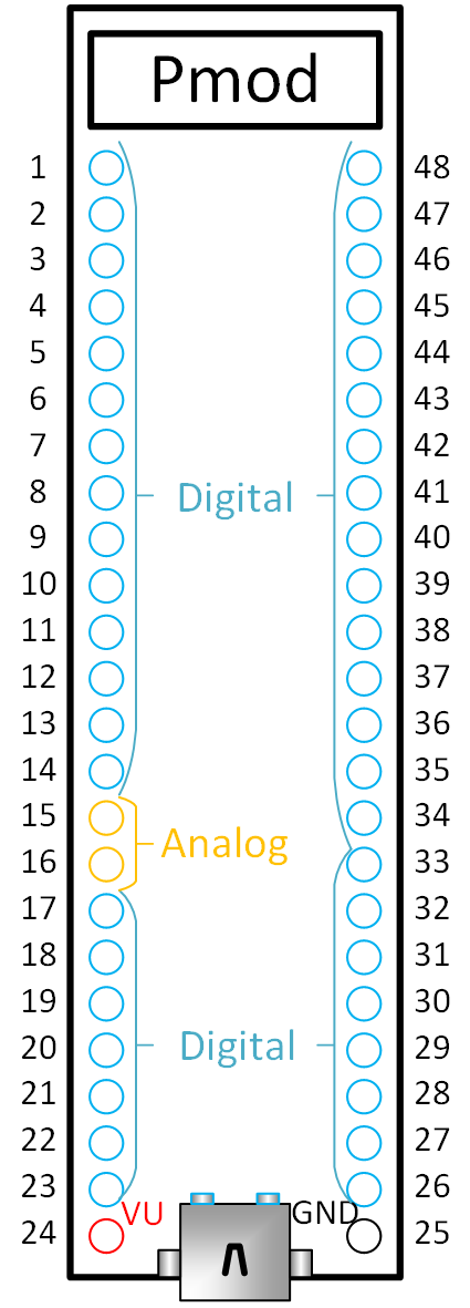
Figure 8.1. DIP Pin diagram
VU (pin 24) can be used to power the Cmod A7 when it is not connected to a USB host. When the device is connected to a USB host, VU is driven by the 5V rail of the USB connector and can be used to power devices external to the Cmod A7. See the “Power” section of this manual for more information on powering the Cmod A7.
8.1 DIP Digital I/O
The pins connected directly to the FPGA can be used as general purpose inputs or outputs. There are no series resistors between the FPGA and the DIP pins, so care should be taken not to cause shorts or connect them to voltages greater than allowed by the FPGA. The absolute maximum voltages for these pins are outlined in Table 8.1.
| Absolute Minimum Voltage | Recommended Minimum Operating Voltage | Recommended Maximum Operating Voltage | Absolute Maximum Voltage | |
|---|---|---|---|---|
| Powered from USB or VU | -0.4 V | -0.2 V | 3.4 V | 3.75 V |
| Unpowered | -0.4 V | N/A | N/A | 0.55 V |
Table 8.1. DIP Pin Voltage Ratings
For more information on the electrical characteristics of the pins connected to the FPGA, please see the Artix 7 datasheet from Xilinx.
8.2 Analog Inputs
Pins 15 and 16 of the DIP connector are used as analog inputs to the XADC module of the FPGA. The FPGA expects that the inputs range from 0-1 V, so we use an external circuit to scale down the input voltage from 3.3V. This circuit is shown in Figure 8.2.1. This circuit allows the XADC module to accurately measure any voltage between 0V and 3.3V (relative to GND on pin 25) that is applied to either of these pins.
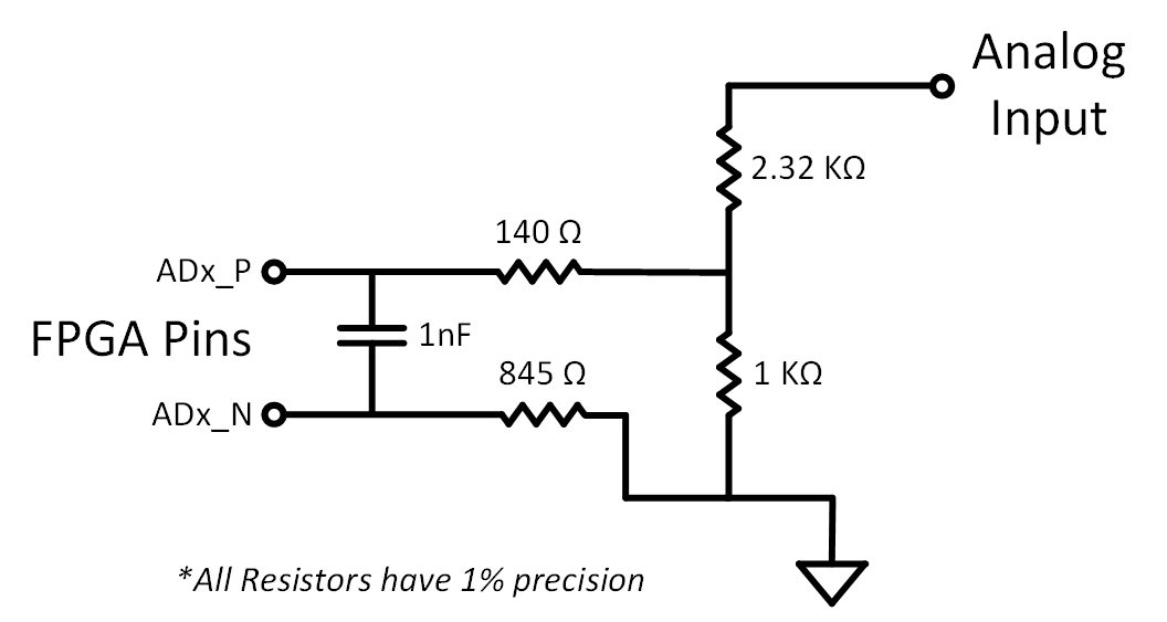
Figure 8.2.1. Analog Input Circuit
The XADC core within the Artix-7 is a dual channel 12-bit analog-to-digital converter capable of operating at 1 MSPS. Either channel can be driven by any of the two auxiliary analog inputs connected to the DIP pins. The XADC core is controlled and accessed from a user design via the Dynamic Reconfiguration Port (DRP). The DRP also provides access to voltage monitors that are present on each of the FPGA’s power rails, and a temperature sensor that is internal to the FPGA. For more information on using the XADC core, refer to the Xilinx document titled 7 Series FPGAs and Zynq-7000 All Programmable SoC XADC Dual 12-Bit 1 MSPS Analog-to-Digital Converter. A demo that uses the XADC core is available on the Cmod A7 resource center.
9 Pmod Connector
Pmod connectors are 2×6, right-angle, 100-mil spaced female connectors that mate with standard 2×6 pin headers. Each 12-pin Pmod connector provides two 3.3V VCC signals (pins 6 and 12), two Ground signals (pins 5 and 11), and eight logic signals, as shown in Fig. 9.1. The VCC and Ground pins can deliver up to 1A of current, but care must be taken not to exceed any of the power budgets of the onboard regulators or the external power supply (these are described in the “Power supplies” section).
Warning: Since the Pmod pins are connected to Artix-7 FPGA pins using a 3.3V logic standard, care should be taken not to drive these pins over 3.4V.
Digilent produces a large collection of Pmod accessory boards that can attach to the Pmod expansion connectors to add ready-made functions like A/D’s, D/A’s, motor drivers, sensors, and other functions. See www.digilentinc.com for more information.
The Cmod A7 has one “standard” type Pmod connector, and the FPGA pin connections for it are described in Table 9.1. Standard Pmod connectors are connected to the FPGA via 200 Ohm series resistors. The series resistors prevent short circuits that can occur if the user accidentally drives a signal that is supposed to be used as an input. The downside to this added protection is that these resistors can limit the maximum switching speed of the data signals.
 Figure 9.1. Pmod Diagram
| Pmod JA | |
|---|---|
| Pmod Type | Standard |
| Pin 1 | G17 |
| Pin 2 | G19 |
| Pin 3 | N18 |
| Pin 4 | L18 |
| Pin 7 | H17 |
| Pin 8 | H19 |
| Pin 9 | J19 |
| Pin 10 | K18 |
Table 9.1. Cmod A7 Pmod Pinout