Pmod DA1 Reference Manual
The Pmod DA1 is retired and no longer for sale in our store.
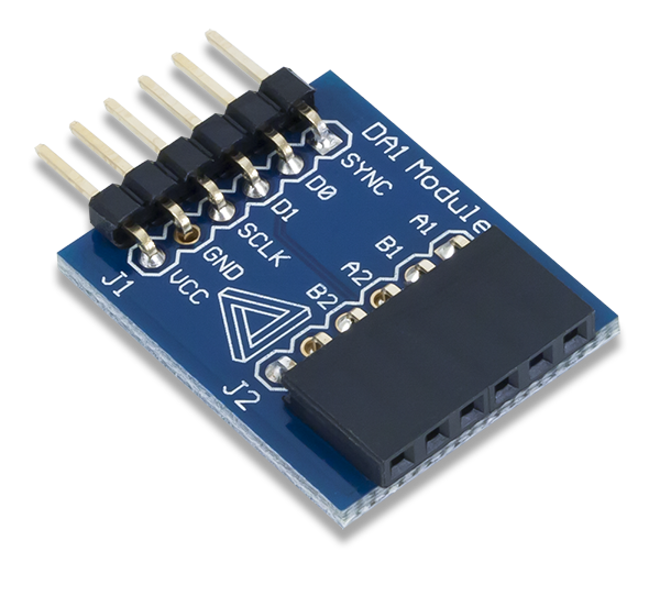
The Digilent Pmod DA1 (Revision C) is an 8-bit Digital-to-Analog Converter module that can output up to four different analog signals simultaneously. This module is ideal for users who want to output a variable voltage signal but do not want to use up their system board's analog capable pins.
Download This Reference Manual
Features
- Two 8-bit DACs
- Four D/A conversion channels
- Maximum conversion rate of 1.875 MSa
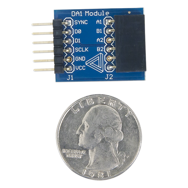
- Small PCB size for flexible designs 1.0“ × 0.8” (2.5 cm × 2.0 cm)
- 6-pin Pmod connector with GPIO interface
Functional Description
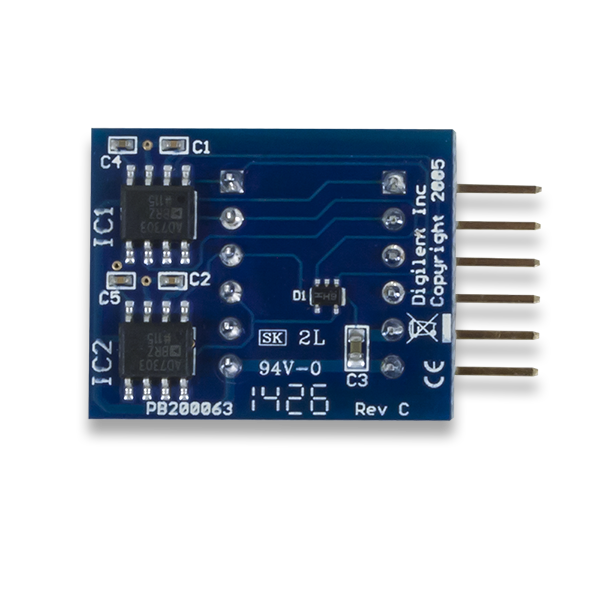
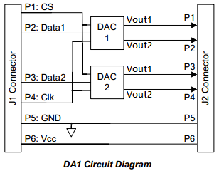
The Pmod DA1 converts an 8-bit digital input signal to a corresponding analog output voltage ranging from 0 to Vdd. Each of the two AD7303 on this Pmod have two 8-bit DACs allowing the user to select which DAC they want their stream of data to be passed through. Because each chip is double buffered, users may also choose to send two separate streams of data on an input and then update each of the corresponding outputs simultaneously.
Interfacing with the Pmod
The Pmod DA1 communicates with the host board via an SPI-like communication protocol. The difference between the standard SPI protocol and this protocol is manifested in the pin arrangement on this Pmod. A typical SPI interface would expect a Chip Select, a Master-Out-Slave-In, a Master-in-Slave-Out, and a Serial Clock signal. However, with the two DACs on this chip both of the data lines, MOSI and MISO, are designed to operate only as inputs, making them both Master-Out-Slave-In data lines.
The Pmod DA1 will receive its 8 bits of information from the system board through 16 clock cycles with first eight bits consisting of eight control bits and the remaining eight bits representing the 8 bits of the data with the MSB first. The each bit is received by the rising edge of the serial clock line. The function dictated by the first eight control bits is executed when the chip select line is brought high.
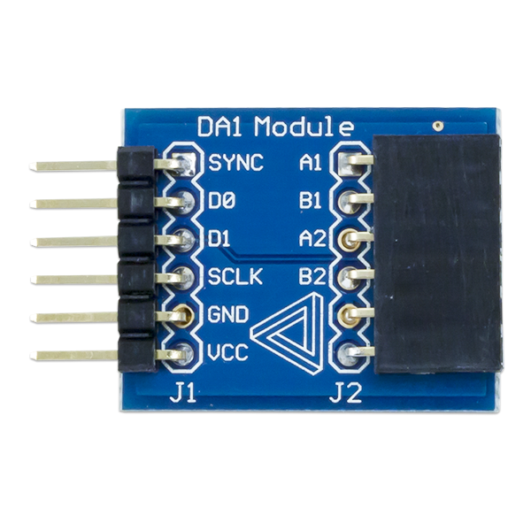
A pinout table and diagram for the Pmod DA1 are provided below:
| Pin Descriptions for the PmodDA1 | ||||||
|---|---|---|---|---|---|---|
| Header J1 | Header J2 | |||||
| Pin | Signal | Description | Pin | Signal | Description | |
| 1 | ~SYNC | Chip Select (active low) | 1 | A1 | Output Data A1 | |
| 2 | D0 | Input Data 1 | 2 | B1 | Output Data B1 | |
| 3 | D1 | Input Data 2 | 3 | A2 | Output Data A2 | |
| 4 | SCK | Serial Clock | 4 | B2 | Output Data B2 | |
| 5 | GND | Power Supply Ground | 5 | GND | Power Supply Ground | |
| 6 | VCC | Power Supply (3.3V) | 6 | VCC | Positive Power Supply | |
Table 1 Connector J1- Pin Descriptions as labeled on the Pmod
The on-board DACs can in principle use either an external or internal reference voltage; however, the Pmod DA1 is designed that the internal reference voltage of Vdd/2 volts must be used. Because of this, the first bit in the command signal sent to the Pmod must always be a logic low signal in order to use the internal reference voltage on the DAC. Tables describing the command signal and the associated bits from the AD7303 datasheet are provided below.
| PmodDA1 Input Shift Register Structure | |||||||||||||||
|---|---|---|---|---|---|---|---|---|---|---|---|---|---|---|---|
| Control bits | Data Bits | ||||||||||||||
| ~INT/EXT | X | LDAC | PDB | PDA | ~A/B | CR1 | CR0 | DB7 | DB6 | DB5 | DB4 | DB3 | DB2 | DB1 | DB0 |
| (MSB) | (LSB) | ||||||||||||||
Note* The “~” signifies that the signal is active when driven low
| Bit Descriptions | |
|---|---|
| Bit Name | Description |
| ~INT/EXT | Selects between the internal and external voltage reference |
| X | Don't Care |
| LDAC | Load DAC bit to both load and update the DAC outputs |
| PDB | Power-down DAC B |
| PDA | Power-down DAC A |
| ~A/B | Selects either DAC A or DAC B to process the data |
| CR1 | Works with CR0 as per the Control Bits Truth Table below |
| CR0 | Works with CR1 as per the Control Bits Truth Table below |
| Data | The user submitted data where DB7 is the MSB and DB0 is the LSB |
| Control Bits Truth Table | ||||
|---|---|---|---|---|
| LDAC | ~A/B | CR1 | CR0 | Resulting Operation |
| 0 | X | 0 | 0 | Both DAC registers loaded from the shift register |
| 0 | 0 | 0 | 1 | Update DAC A register from the shift register |
| 0 | 1 | 0 | 1 | Update DAC B register from the shift register |
| 0 | 0 | 1 | 0 | Update DAC A DAC register from the input register |
| 0 | 1 | 1 | 0 | Update DAC B DAC register from the input register |
| 0 | 0 | 1 | 1 | Update DAC A DAC register from the shift register |
| 0 | 1 | 1 | 1 | Update DAC B DAC register from the shift register |
| 1 | 0 | X | X | Load DAC A input register from the shift register and update both DAC registers |
| 1 | 1 | X | X | Load DAC B input register from the shift register and update both DAC registers |
| Another Truth Table compiled from the AD7303 Datasheet | |||||
|---|---|---|---|---|---|
| PDA | PDB | Description | ~INT/EXT | Description | |
| 0 | 0 | Both DACs are Active | 0 | Internal Vdd/2 reference voltage selected | |
| 0 | 1 | DAC A is active and DAC B is in power-down mode | 1 | External reference voltage selected | |
| 1 | 0 | DAC B is active and DAC A is in power-down mode | |||
| 1 | 1 | Both DACs are in power-down mode | |||
Any external power applied to the Pmod DA1 must be within 2.7V and 5.5V; however, it is recommended that Pmod is operated at 3.3V.
Physical Dimensions
The pins on the pin header are spaced 100 mil apart. The PCB is 1 inch long on the sides parallel to the pins on the pin header and 0.8 inches long on the sides perpendicular to the pin header.
Additional Information
The schematics of the Pmod DA1 are available here. The datasheet for Analog Devices AD7303 which is used in this Pmod is available here.
Example code demonstrating how to get information from the Pmod DA1 can be found here.
If you have any questions or comments about the Pmod DA1, feel free to post them under the appropriate section (“Add-on Boards”) of the Digilent Forum.

