Pmod CLP Reference Manual
Note
The Pmod CLP is retired and no longer for sale in our store.
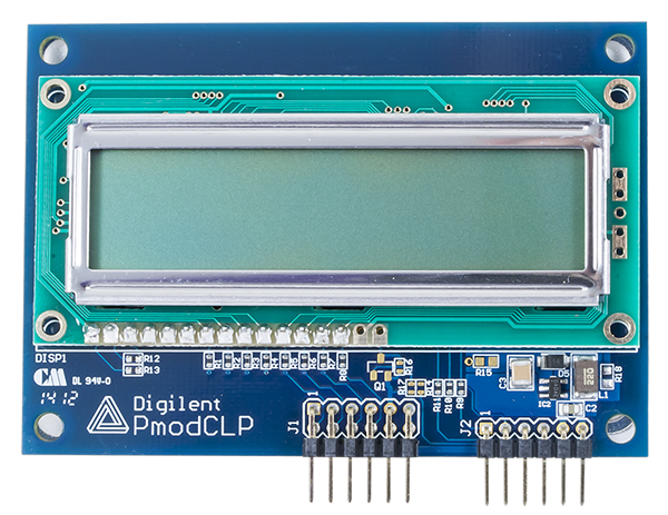
The Digilent Pmod CLP (Revision B) is a 16×2 character LCD module that uses a 8-bit parallel data interface to let system boards display up to 32 different characters out of over 200 possible options.


Download This Reference Manual
Features
- 16×2 character LCD with parallel interface
- 192 predefined characters including 93 ASCII characters
- Up to 8 user-definable characters
- Read and write capability to and from the display
Functional Description
The Pmod CLP utilizes a Samsung KS0066 LCD controller to display information to a Sunlike LCD panel. The module can execute a variety of instructions, such as erasing specific characters, setting different display modes, scrolling, and displaying user-defined characters.
Interfacing with the Pmod
The Pmod CLP communicates with the host board via the GPIO protocol. This particular module requires specific timings in order to program the KS0066 correctly, as per the KS0066 datasheet. These timings are described after the pinout description table shown below:
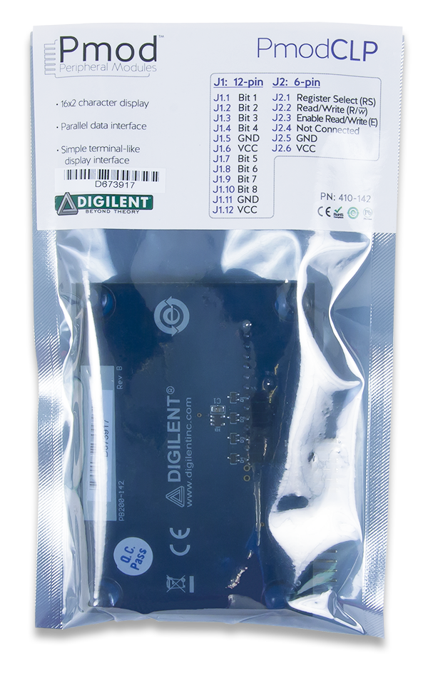
Pinout Description Table
| Pmod CLP Connector Signals | ||||||||||
|---|---|---|---|---|---|---|---|---|---|---|
| Header J1 - Top Half | Header J1 - Bottom Half | Header J2 | ||||||||
| Pin | Signal | Description | Pin | Signal | Description | Pin | Signal | Description | ||
| 1 | DB0 | Data Bit 0 | 7 | DB4 | Data Bit 4 | 1 | RS | Register Select: High for Data Transfer, Low for Instruction Transfer | ||
| 2 | DB1 | Data Bit 1 | 8 | DB5 | Data Bit 5 | 2 | R/W | Read/Write signal: High for Read mode, Low for Write mode | ||
| 3 | DB2 | Data Bit 2 | 9 | DB6 | Data Bit 6 | 3 | E | Read/Write Enable: High for Read, falling edge writes data | ||
| 4 | DB3 | Data Bit 3 | 10 | DB7 | Data Bit 7 | 4 | NC | Optional back-light enable (not connected on the Pmod CLP | ||
| 5 | GND | Power Supply Ground | 11 | GND | Power Supply Ground | 5 | GND | Power Supply Ground | ||
| 6 | VCC | Positive Power Supply¹ | 12 | VCC | Positive Power Supply¹ | 6 | VCC | Positive Power Supply¹ | ||
¹For Revision A of the Pmod CLP this must be at 5V. For Revision B, this must be at 3.3V

Timing Requirements
After power-on, at least 20ms must elapse before the “Function Set” instruction code can be written to set the bus width, number of lines, and character patterns (8-bit interface, 2 lines, and 5×8 dots are appropriate). After the Function Set instruction, at least 37us must elapse before the “Display On/Off Control” instruction can be written (to turn the display on, turn the cursor on or off, and set the cursor to blink or no blink). After another 37us, the “Clear Display” instruction can be issued.
After another 1.52ms, the “Entry Mode Set” instruction can set address increment (or address decrement) mode, and display shift mode (on or off). After this sequence, data can be written into the DDRAM via the “Write data into RAM” to cause information to appear on the display. Note that other compatible LCD controllers use similar start-up sequences which may not use the same timings as the Samsung controller.
The table below lists the required bit order needed in order to send a variety of instructions to the LCD controller on the Pmod CLP. Before the 8 bits of parallel data (DB7 through DB0) are sent, the output enable pin, E, must be brought to a high '1' state and then brought to a low '0' state at end of the sequence in order to transfer the data bits to the LCD controller.
Pmod CLP Instruction Codes
| LCD Instructions and Codes | |||||||||||
|---|---|---|---|---|---|---|---|---|---|---|---|
| Instruction | Instruction bit assignments | Description | |||||||||
| RS | R/W | DB7 | DB6 | DB5 | DB4 | DB3 | DB2 | DB1 | DB0 | ||
| Clear Display | 0 | 0 | 0 | 0 | 0 | 0 | 0 | 0 | 0 | 1 | Clear display by writing a 20H to all DDRAM locations; set DDRAM address register to 00H; and return cursor to home. |
| Return Home | 0 | 0 | 0 | 0 | 0 | 0 | 0 | 0 | 1 | X | Return cursor to home (upper left corner), and set DDRAM address to 0H. DDRAM contents not changed. |
| Entry Mode Set | 0 | 0 | 0 | 0 | 0 | 0 | 0 | 1 | I/D | SH | I/D = '1' for right-moving cursor and address increment; SH = '1' for display shift (direction set by I/D bit). |
| Display On/Off Control | 0 | 0 | 0 | 0 | 0 | 0 | 1 | D | C | B | Set display (D), cursor (C), and blinking cursor (B) on or off. |
| Cursor or Display shift | 0 | 0 | 0 | 0 | 0 | 1 | S/C | R/L | X | X | S/C = '0' to shift cursor right or left, '1' to shift entire display right or left (R/L = '1' for right). |
| Function Set | 0 | 0 | 0 | 0 | 1 | DL | N | F | X | X | Set interface data length DL ('1' for 8 bit), number of display lines N ('1' for 2 lines), font F ('0' for 5×8 dots) |
| Set CGRAM Address | 0 | 0 | 0 | 1 | AC5 | AC4 | AC3 | AC2 | AC1 | AC0 | Set CGRAM address counter AC5 - AC0 |
| Set DDRAM Address | 0 | 0 | 1 | AC6 | AC5 | AC4 | AC3 | AC2 | AC1 | AC0 | Set CGRAM address counter AC5 - AC0 |
| Read busy flag/address | 0 | 1 | BF | AC6 | AC5 | AC4 | AC3 | AC2 | AC1 | AC0 | Read busy flag (BF) and address counter AC6-AC0 |
| Write data to RAM | 1 | 0 | D7 | D6 | D5 | D4 | D3 | D2 | D1 | D0 | Write data into DDRAM or CGRAM, depending on which address was last set |
| Read data to RAM | 1 | 1 | D7 | D6 | D5 | D4 | D3 | D2 | D1 | D0 | Read data into DDRAM or CGRAM, depending on which address was last set |
*Note “X” represents a “don't care” bit
CGRAM and DDRAM
The LCD controller contains a character-generator ROM (CGROM) with 192 preset 5×8 character patterns (see table 4 below), a character-generator RAM (CGRAM) that can hold 8 user-defined 5×8 characters, and a display data RAM (DDRAM) that can hold 80 character codes. Character codes written into the DDRAM serve as indexes into the CGROM (or CGRAM). Writing a character code into a particular DDRAM location will cause the associated character to appear at the corresponding display location. Display positions can be shifted left or right by setting a bit in the Instruction Register (IR). The write-only IR directs display operations (such as clear display, shift left or right, set DDRAM address, etc). A busy flag shows whether the display has competed the last requested operation; prior to initiating a new operation, the flag can be checked to see if the previous operation has been completed.
The display has more DDRAM locations than can be displayed at any given time. DDRAM locations 00H to 27H map to the first display row, and locations 40H to 67H map to the second row. Normally, DDRAM location 00H maps to the upper left display corner (the “home” location, and 40H to the lower left. Shifting the display left or right can change this mapping. The display uses a temporary data register (DR) to hold data during DDRAM /CGRAM reads or writes, and an internal address register to select the RAM location. Address register contents, set via the Instruction Register, are automatically incremented after each read or write operation. The LCD display uses ASCII character codes. Codes up through 7F are standard ASCII (which includes all “normal” alphanumeric characters). Codes above 7F produce various international characters.
The predefined characters available to display (from the KS0066 datasheet) are shown in the table below:
Predefined Character Table

Any external power applied to the Pmod CLP must be at 5V for Revision A of the Pmod CLP and at 3.3V for Revision B of the Pmod CLP.
Physical Dimensions
The pins on the pin header are spaced 100 mil apart. The PCB is 2.3 inches long on the sides parallel to the pins on the pin header and 3.3 inches long on the sides perpendicular to the pin header.
Additional Information
The schematics of the Pmod CLP are available here. Additional information about the display controller can be found by checking out its datasheet here. Similarly, the datasheet on the display itself can be found here.
Example code demonstrating how to get information from the Pmod CLP can be found here.
If you have any questions or comments about the Pmod CLP, feel free to post them under the appropriate section (“Add-on Boards”) of the Digilent Forum.