Pmod SF Reference Manual
Note
The Pmod SF is retired and no longer for sale in our store.
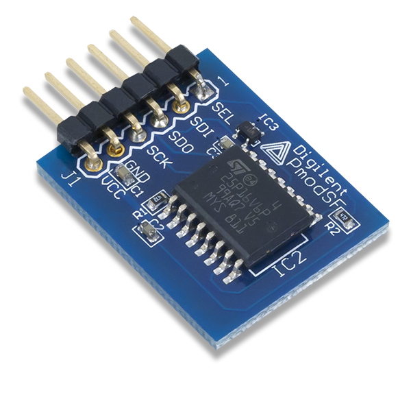
The Digilent Pmod SF (Revision C) is a small serial flash module that helps demonstrate the uses of non-volatile memory.


Download This Reference Manual
Features
- 16Mbit serial Flash memory
- Data retention greater than 20 years
- 6-pin Pmod connector with SPI interface
- Follows Digilent Interface Specification Type 2
Functional Description
The Pmod SF utilizes ST Microelectronics M25P16 which provides 16 Mbits of flash memory that can be accessed through the SPI protocol. Although this amount of memory is very small compared to modern flash drives, the Pmod SF is a great way to get introduced to controlling non-volatile memory and can be easily incorporated into projects that need a way to store some information without using the USB interface.
Interfacing with the Pmod
The Pmod SF communicates with the host board via the SPI protocol. By bringing the Chip Select (CS) line low, users are able to issue a variety of read, write, and erase commands to the memory chip. A table of the available commands for the the M25P16 from its respective datasheet is provided below.
| Instruction | Description | One-Byte Instruction Code | Number of Address Bytes | Number of Dummy Bytes | Number of Data Bytes |
|---|---|---|---|---|---|
| WREN | Write Enable | 0x06 | 0 | 0 | 0 |
| WRDI | Write Disable | 0x04 | 0 | 0 | 0 |
| RDID | Read Identification | 0x9F | 0 | 0 | 1 to 3 |
| RDSR | Read Status Register | 0x05 | 0 | 0 | 1 to ∞ |
| WRSR | Write Status Register | 0x01 | 0 | 0 | 1 |
| READ | Read Data Bytes | 0x03 | 3 | 0 | 1 to ∞ |
| FAST_READ | Read Data Bytes at Higher Speed | 0x0B | 3 | 1 | 1 to ∞ |
| PP | Page Program | 0x02 | 3 | 0 | 1 to 256 |
| SE | Sector Erase | 0xD8 | 3 | 0 | 0 |
| BE | Bulk Erase | 0xC7 | 0 | 0 | 0 |
| DP | Deep Power-down | 0xB9 | 0 | 0 | 0 |
| RES | Release from DP and Read Electronic Signature | 0xAB | 0 | 3 | 1 to ∞ |
| Release from DP | 0 | 0 | 0 |
The address bits range from 0x000000 to 0x1FFFFF, with the first two hexadecimal bits indicating which memory sector the data is located in. Thankfully, users do not have to explicitly worry about writing to and reading from the memory module as there is a library that takes care of these commands for us.

Pinout Description Table
| Pin | Signal | Description |
|---|---|---|
| 1 | ~CS | Chip Select |
| 2 | MOSI | Master-Out-Slave-In |
| 3 | MISO | Master-In-Slave-Out |
| 4 | SCK | Serial Clock |
| 5 | GND | Power Supply Ground |
| 6 | VCC | Positive Power Supply (3.3V) |
Any external power applied to the Pmod SF must be within 2.7V and 3.6V; it is recommended that Pmod is operated at 3.3V.
Physical Dimensions
The pins on the pin header are spaced 100 mil apart. The PCB is 1 inch long on the sides parallel to the pins on the pin header and 0.8 inches long on the sides perpendicular to the pin header.
Additional Information
The schematics of the Pmod SF are available here. Additional information about the flash memory chip including communication modes and specific timings of the chip can be found by checking out its datasheet here.
Example code demonstrating how to get information from the Pmod SF can be found here.
If you have any questions or comments about the Pmod SF, feel free to post them under the appropriate section (“Add-on Boards”) of the Digilent Forum.