Pmod AD5 Reference Manual
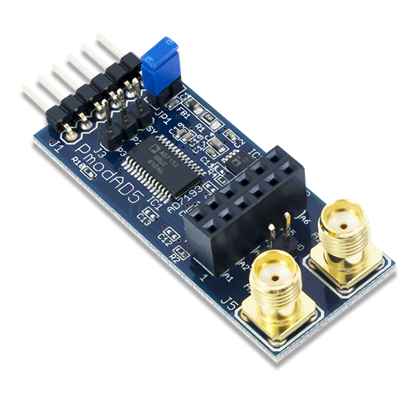
The Digilent PmodAD5 (Revision A) is an analog-to-digital converter (ADC) that utilizes a fourth order Σ-Δ modulator, a programmable gain array, and on-chip digital filtering including a variety of sinc filters and zero latency features, all powered by the Analog Devices AD7193.

Download This Reference Manual
Features
- 24-bit resolution
- 4 differential or 8 pseudo differential input channels
- Simultaneous 50 Hz/60 Hz rejection
Functional Description
The PmodAD5 utilizes Analog Devices AD7193 to provide 4 differential or 8 pseudo differential analog inputs. With 24-bit resolution and rms noise as low as 11 nV, highly accurate voltage measurements can be taken.
Interfacing with the Pmod
The PmodAD5 communicates with the host board via the SPI protocol. By driving the Chip Select line low, users can transfer information to and from the device with the most significant bit (MSB) first.
The default setting of the AD7193 upon power-up is that a single analog-to-digital conversion is made comparing the voltage difference between pins A1 (+) and A2 (-) on header J2. The input voltage that is allowed with the default settings is ±19.53 mV with respect to the on-board reference voltage of 2.5V. Users are able to receive the 24 bits of data by first pulling the chip select line low and waiting the required conversion and settling time (100 ms by default). Users can then write to the communications register to indicate that they want to read the data and then clock in the 24 bits of data from the data register and finally pull the chip select line back to a high voltage state. An example of what the data stream might look like is given below:
| Example Data Stream of the Measured Differential Voltage | |||||||
|---|---|---|---|---|---|---|---|
| Communications Register | |||||||
| ~WEN | R/~W | Data Register Address | CREAD | 0 | 0 | ||
| 0 | 1 | 0 | 1 | 1 | 0 | 0 | 0 |
| Data Register | |||||||
| Read Bits D23-D0 | |||||||
Some users may wish to have a wider voltage range that they are able to analyze than 2.5V ±19.53 mV. This can be adjusted by changing specific values within the Configuration register; namely, the Reference Select bit (D20) and the three gain bits (D2-D0).
An example bit stream that changes the Reference Select bit from the default reference of 2.5V to the user supplied reference voltage between pins REFIN2+ and REFIN2- and changes the gain from the default of 128 to 1 is provided below:
| Example Data Stream of the Measured Differential Voltage | |||||||
|---|---|---|---|---|---|---|---|
| Communications Register | |||||||
| ~WEN | R/~W | Configuration Register Address | CREAD | 0 | 0 | ||
| 0 | 0 | 0 | 1 | 0 | 0 | 0 | 0 |
| Configuration Register (first 8 of 24 bits) | |||||||
| Chop | 0 | 0 | REFSEL | 0 | Pseudo | Short | TEMP |
| 0 | 0 | 0 | 1 | 0 | 0 | 0 | 0 |
| Configuration Register (second 8 of 24 bits) | |||||||
| Channel Enable bits for CH7 - CH0 | |||||||
| 0 | 0 | 0 | 0 | 0 | 0 | 0 | 1 |
| Configuration Register (last 8 of 24 bits) | |||||||
| Burn | REFDET | 0 | BUF | U/~B | G2 | G1 | G0 |
| 0 | 0 | 0 | 1 | 0 | 0 | 0 | 0 |
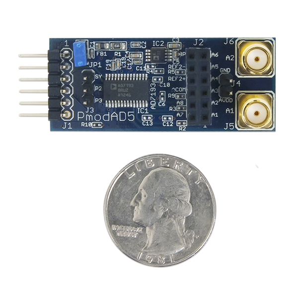
Pinout Description Table
| Pmod Header J1 | Pmod Header J2 (note that pin 1 is on the lower-right hand corner of the header) | ||||||||
|---|---|---|---|---|---|---|---|---|---|
| Pin | Signal | Description | Pin | Signal | Description | Pin | Signal | Description | |
| 1 | CS | Chip Select | 1 | A1 | Analog Input 1 | 7 | A7 | Analog Input 7 | |
| 2 | MOSI | Master-Out-Slave-In | 2 | A2 | Analog Input 2 | 8 | A8 | Analog Input 8 | |
| 3 | MISO | Master-In-Slave-Out | 3 | A3 | Analog Input 3 | 9 | AINCOM | Common Analog Input | |
| 4 | SCK | Serial Clock | 4 | A4 | Analog Input 4 | 10 | REFIN2+ | Reference Input 2 + | |
| 5 | GND | Power Supply Ground | 5 | A5 | Analog Input 5 | 11 | REFIN2- | Reference Input 2 - | |
| 6 | VCC | Power Supply (3.3V/5V) | 6 | A6 | Analog Input 6 | 12 | BPDSW | Bridge Power-Down Switch | |
Any incoming input voltage to be measured must be within ±(AVDD-1.25V)/gain. As AVDD must be within 3V and 5.25V, if a 5V power supply is used, the largest possible range of incoming input voltage is -3.75V to 3.75V. By default, the jumper on JP1 is loaded such that the AVDD voltage matches the DVDD voltage. If users want to apply a higher AVDD voltage to header J4 so that they are able to utilize larger reference voltages, the jumper block from JP1 must be removed so that the two voltage sources are disconnected.
Any external power applied to the PmodAD5 must be within 3V and 5.25V; however, it is recommended that Pmod is operated at 3.3V.
Physical Dimensions
The pins on the pin header are spaced 100 mil apart. The PCB is 1.9 inches long on the sides parallel to the pins on the pin header and 0.8 inches long on the sides perpendicular to the pin header.
Additional Information
The schematics of the PmodAD5 are available here. Additional information about the ADC including communication modes and specific timings of the chip can be found by checking out its datasheet here.
More specific information about how to use the PmodAD5 including how to setup the simultaneous 50 Hz/60 Hz rejection can be found by checking out our user guide. Example code demonstrating how to get information from the PmodAD5 can be found here.
If you have any questions or comments about the PmodAD5, feel free to post them under the appropriate section (“Add-on Boards”) of the Digilent Forum.