Getting Started with the Nexys4DDR
What's in the Box?

Powering it On
To power on the Nexys4DDR, you will need a micro-USB cable. Plug this cable into the JTAG slot on the Nexys4DDR, plug the other end into your computer, and flip the power switch to the “On” position. This will begin the out of box demo.
More information on this startup demo can be found here.
Getting Started with Vivado
The files needed for this demo can be downloaded by clicking here. You'll also need the constraints file. The constraint file is dependent on the development environment. For ISE designs the UCF file can be downloaded here. For Vivado designs, the XDC file can be downloaded here.
More information on the Abacus project can be found here.
Download and Install Vivado
First, install the latest version of Vivado by following our guide here.
Creating a Project
Now that we have Vivado 14.3 installed, we're going to create a project.

This opens Vivado's New Project wizard. Click “Next” and you'll see this screen.

Name your project (no spaces!) and choose your project saving directory before clicking “Next”. You will now see this screen.
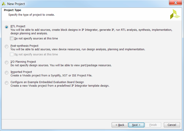
Select RTL Project and click “Next”
In this window, you can select any other source files or directories that you'll want to use in your projects. We can also select which language we'll be programming in.
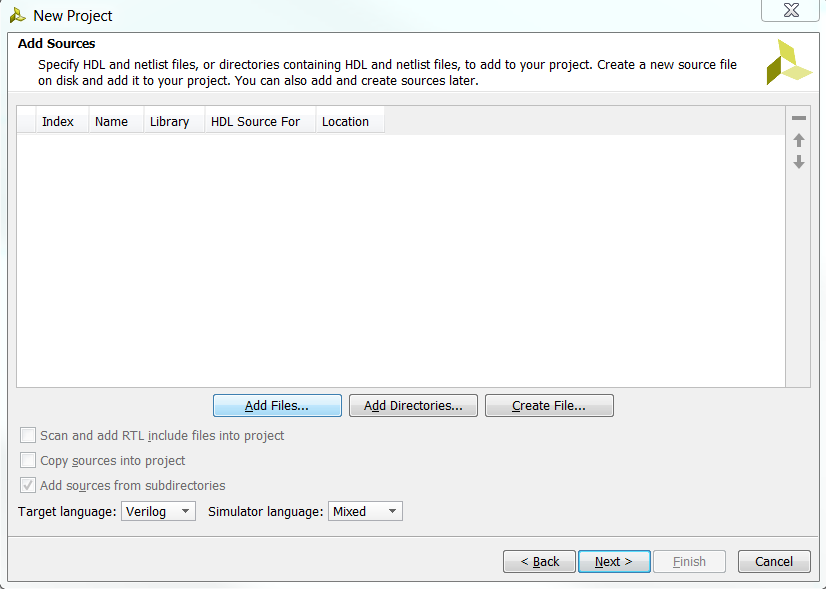
We'll be importing the pre-built Verilog files so click “Add Files”, navigate to where you saved the project files from before, and select them all. It should be noted that if you check the “Copy sources into project” box, Vivado will create separate copies of these sources and place them within your project directory. Click “Next”.
This window lets you choose existing IPs (Intellectual Property) cores if you have them.
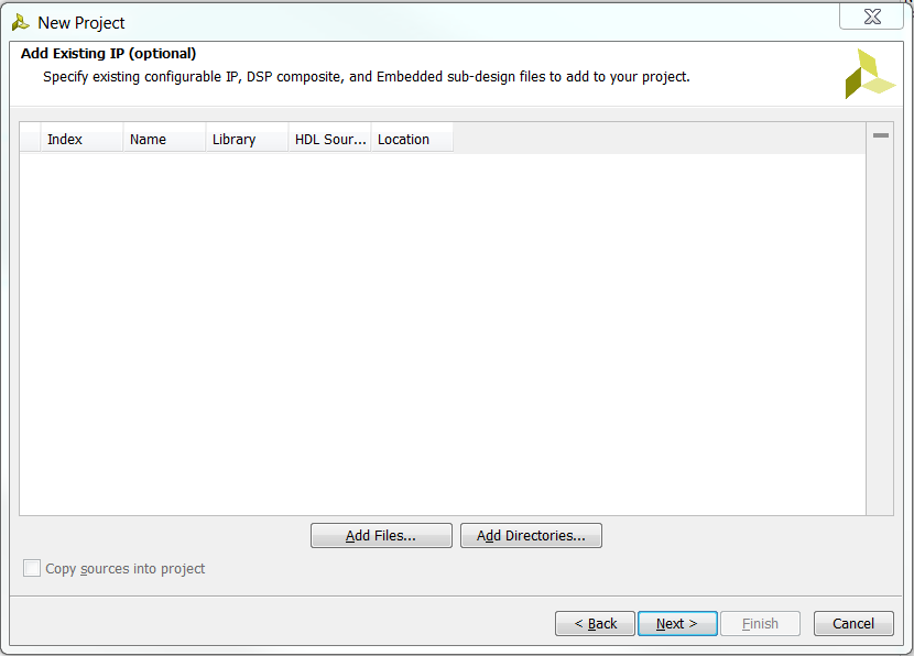
Click “Next” and you'll see this window.

This is where we'll import our Xlilinx Design Constraints file (XDC) to map the HDL signals to the Artix-7 pins. Click on “Add Files”, navigate to where you saved your Nexys4DDR_Master.xdc file, select it, and click “Next”.

At this point you'll see the part selection screen. To find our board set the following filters
Family: Artix-7
Sub-Family: Artix-7
Package: csg324
Speed grade: -1
Select the part labeled “xc7a100tcsg324-1” and click “Next” followed by finish.

You'll find all of the information you need on the Artix-7 chip on your board.

This will create your project and bring you to the Vivado project home page.
Working with Vivado

On the home page, you will see the files that you imported earlier in the “Sources” box.

Double clicking a file will open it in the window to the right. “Nexys4_Abacus_Top” is the top module for the abacus demo we will be running. Clicking the [+] button will reveal the lower level modules used in it.

Before we run our program, we must first map the signals to pins using the Nexys4DDR_Master.xdc file we imported. To do this, we will open Nexys4DDR_Master.xdc. Inside this file, we will see how Vivado maps signals to pins. Each line should be commented out at this point (with #), so it should look something like this.

First, we want to make sure our signal names match the ones in the .xdc file. This can be confirmed by comparing the signal name in the .xdc file with the signal name in the top module. These are case sensitive!
.xdc file

Top module file

Once these are confirmed, we will uncomment whichever constraints we are using in the .xdc file. These constraints can be uncommented by selecting the lines of the signals we are using and un-toggling the comments (Ctrl+/). In this case, we are using clk, btnC, btnU, btnD, btnR, btnL, sw[0] through sw[15], led[0] through led[15], seg[0] through seg[6], an[0] through an[7], and dp. Go through the xdc file and uncomment the lines corresponding to these signals.

After uncommenting the xdc file, save it and we can start programming your Nexys4DDR.
Programming the Nexys4DDR
There are two ways to program your Nexys4DDR FPGA: using a .bit file and using a .bin file. Using a .bit file, we use the JTAG programming cable to load the bit file into the FPGA. Programming with a .bin file will use the QSPI to program the FPGA each time it is powered on. This means you will not have to reprogram it using the JTAG connector each time. We will specify that we want to generate a .bin file by clicking Tools>Project Settings>Bitstream. In this window we will check the box next to .bin_file.

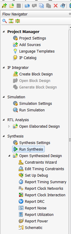
To begin, we will run the synthesis by clicking “Run Synthesis” beneath Synthesis in the Flow Navigator on the left side of Vivado.
When it is done synthesizing your project, you will see the Synthesis Completed window.
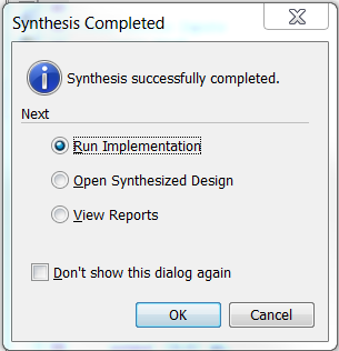
Click “Open Synthesized Design” and then press Ok. You may get several warnings after this, but this just refers to the parts of the Nexys4DDR master XDC file that weren't implemented by our HDL design. It is good practice to only uncomment signal pins that are being used by the design, but this will not affect us in the end.
You should now see this window

Setting device properties (Recommended)
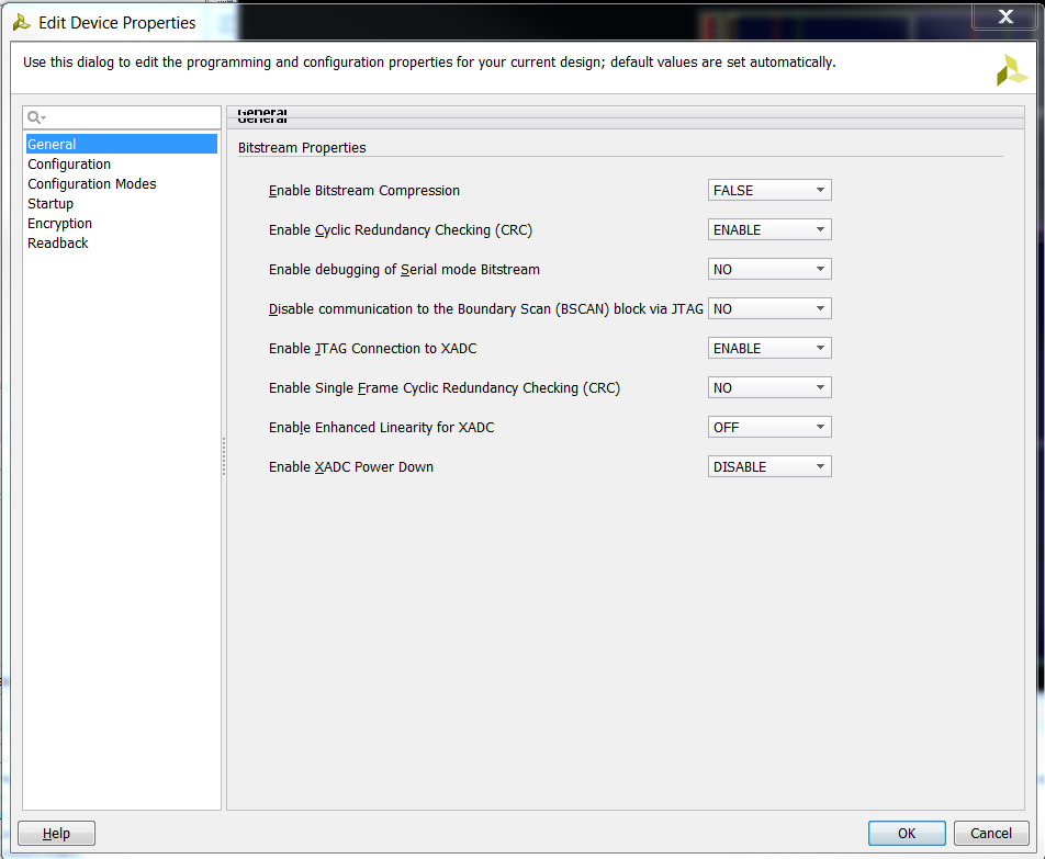
To improve programming speed and avoid programming errors, in the main toolbar select Tools>Edit Device Properties…
Under General, set Enable Bitsream Compression to “TRUE”.
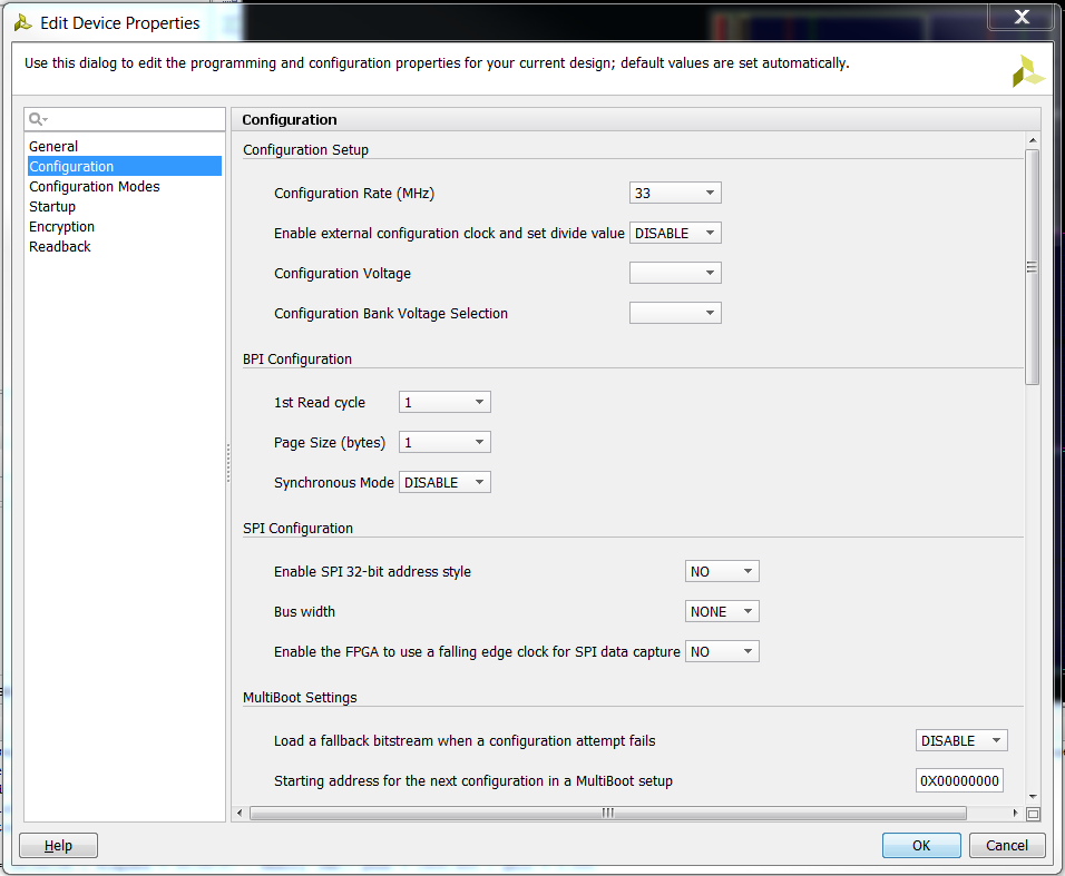
 Under Configuration, set Configuration Rate (Mhz) to 33.
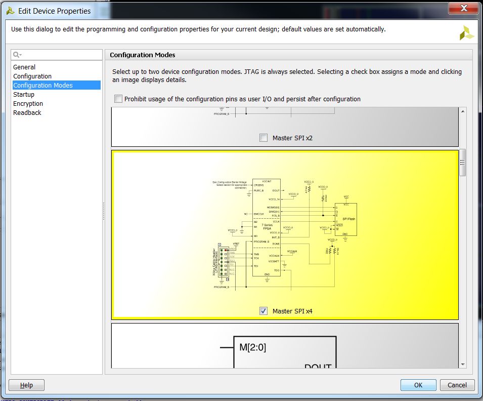
 Under Configuration Modes, select Master SPI x4
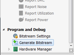
Press Ok, save your synthesized design (Ctrl+S) and then click “Generate Bitstream” in the Flow Navigator on the left side.
 This will open a box stating that you have not implemented your design.
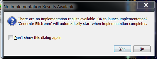 Click “Ok” and Vivado will generate your .bit file and will show you this box.
 Click Open Hardware Manager and click OK.
You will see this screen.
 At this point, make sure your Nexys4DDR is plugged in via USB and turned on. Now click Next twice and you will see this screen.
 Set the JTAG Clock Frequency to 30000000, select the device, and click “Next” followed by “Finish”.
Programming the Nexys4DDR using a .bit file
First, make sure that the jumper JP1 is in the JTAG position.
You should see something like this.
 Click “Program device” (in the green bar) then xc7a35t_0, select your .bit file in the bitstream file box, and click Program.
 This will program your Nexys4DDR through the JTAG connector.
Programming the Nexys4DDR using .bin file
First, make sure the jumper on JP1 is in the QSPI position
In the Hardware Manager window, under hardware right click your device and click Add Configuration Memory Device…
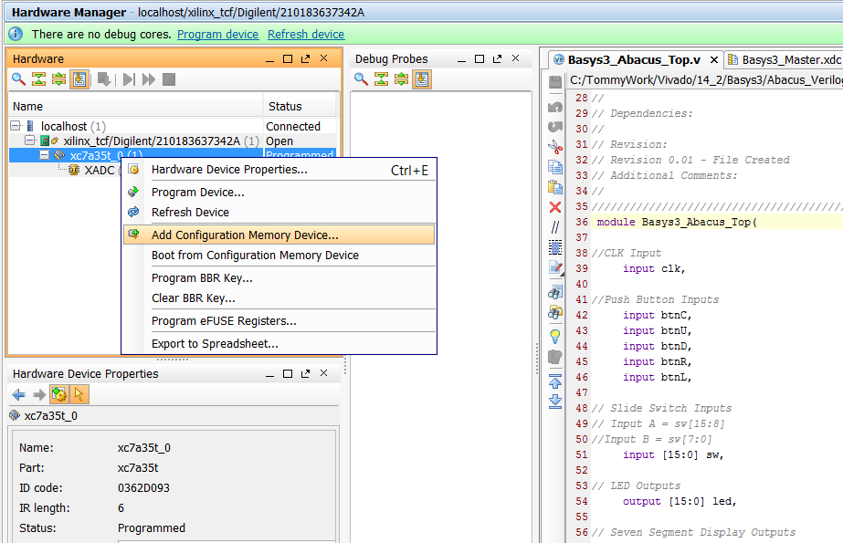 This window will pop up. Search for “Spansion” and select s25fl128sxxxxxx0-spi-x1_x2_x4 (highlighted below). Click OK on the next window asking if you want to program the configuration memory device.

Select the .bin file where it asks for a configuration file and finally click OK.

Vivado will now erase the old configuration file, and reprogram your Nexys4DDR with the Abacus demo file. From now on, when you power cycle the Nexys4DDR, the abacus demo will load at startup.