Cerebot 32MX4 Reference Manual
The Cerebot 32MX4 is now retired and no longer for sale in our store.
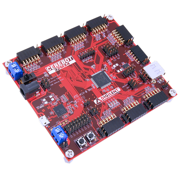
The Cerebot 32MX4 is designed for embedded control and robotic applications as well as microprocessor experimentation. Firmware suitable for many applications can be downloaded to the Cerebot 32MX4's programmable PIC32 microcontroller. The board has a number of connection options and is specially designed to work with the Digilent line of Peripheral Modules (Pmods) with various input and output functions including direct connection of up to 8 RC hobby servos, provides two on-board push-buttons, and four on-board LEDs for user I/O, as well as providing connections for two I2C buses. A serial EEPROM and a serial D/A converter are provided on one of the I2C buses.

Features
- PIC32MX460F512L microcontroller
- Support for programming and debugging within the Microchip MPLAB development environment
- Nine Pmod connectors for Digilent peripheral module boards
- Eight hobby RC servo connectors
- USB 2.0 Device, Host, and OTG support
- Two push buttons
- Four LEDs
- Multiple power supply options, including USB powered
- ESD protection and short circuit protection for all I/O pins
- 512KB internal program flash memory
- 32KB internal SRAM memory
- USB 2.0 compliant full-speed On-The-Go (OTG) controller with dedicated DMA channel
- Two serial peripheral interfaces (SPI)
- Two UART serial interfaces
- Two I2C serial interfaces
- Five 16-bit timer/counters
- Five timer capture inputs
- Five compare/PWM outputs
- Sixteen 10-bit analog inputs
- Two analog comparators
Functional Description
The Cerebot 32MX4 is designed for embedded control and robotic applications as well as microprocessor experimentation. Firmware suitable for many applications can be downloaded to the Cerebot 32MX4's programmable PIC32 microcontroller.
The board has a number of connection options and is specially designed to work with the Digilent line of Peripheral Modules (Pmods) with various input and output functions. For more information, visit the Pmod category. In addition to the Pmod ports, the board supports direct connection of up to 8 RC hobby servos, provides two on-board push-buttons, and four on-board LEDs for user I/O, as well as providing connections for two I2C buses. A serial EEPROM and a serial D/A converter are provided on one of the I2C buses.
The Cerebot 32MX4 can be used with the Microchip MPLAB development environment. In-system-programming and debug of firmware running on the PIC32 part is supported via USB within MPLAB. The in-system-programming and debug subsystem is implemented in IC5, a PIC18LF4550 microcontroller. Access to this subsystem is accomplished via USB connector J11. Normally, J11 will be connected to an available USB port on a PC while developing firmware to run on the PIC32 microcontroller.
The Cerebot 32MX4 features a flexible power supply routing system with a number of options for powering the board as well as powering Pmods connected to the board. It can be USB-powered via either the debug USB port, the USB device port, an external power supply, or batteries.
Programming and In-system Debug Using MPLAB
The Cerebot 32MX4 board is intended to be used with the Microchip MPLAB IDE for firmware development, programming, and in-system debug. The board is compatible with the Microchip PIC32 Starter Kit board, and appears to MPLAB as a PIC32MX Starter Kit. When installing the MPLAB software, ensure that the PIC32MX Starter Kit support is installed.
After the MPLAB software is installed, the first time that the board is used, Windows will need to install the Microchip USB device driver to connect to the board. If the “Found New Hardware Wizard” asks for the installation CD and no CD is available, click OK anyways. In the “Files Needed” dialog box, use the browse button to navigate to the folder: “Program Files\Microchip\MPLAB IDE\PIC32MXSkit\Drivers” and select the file: mp32mxsk.sys and clock on OK. The wizard should then complete installing the proper driver for the board. This process may need to be repeated if the board is later connected to a different USB port.
When creating a new project, ensure that the device is set to PIC32MX460F512L. On the Debugger Select Tool menu, select the PIC32 Starter Kit as the debugger.
Board Power Supply
The Cerebot 32MX4 may be USB powered via either the USB debug port, or the USB device port. Alternatively, the board may be powered via dedicated external power supply connectors.
There are three different power supply connectors on the Cerebot 32MX4 for connecting an external power supply: J13, J14, and J18.
The barrel connector, J13, is useful for desktop development and testing where using USB or battery power is not suitable. J13 is the connector used by the AC supply adapter optionally available from Digilent, or other sources. J13 is a 2.5mm x 5.5mm coaxial connector wired with the center terminal as the positive voltage.
J14 is a two-pin male header that provides easy batter or battery-pack connection. Digilent has both two-cell and four-cell AA battery holders with two-pin connectors available for connection to J14.
J18 is a screw terminal connector for an alternative power supply connection for use with higher current battery packs, bench supplies, or other power sources where use of a hard-wired power supply is desirable.
The Cerebot 32MX4 is rated for external power from 3.6-5V DC. Using voltages outside fo this range could damage the board and connected devices.
Connectors J13, J14, and J18 are wired in parallel and connect to the “External Power” position (center position) on the Power Select jumper block J12. A shorting block should be placed on the “External Power” position of J12 when using this option for board power. Only one of these three power connectors should be used at a time. If multiple power supplies are connected simultaneously, damage to the board or the power supplies may occur.
The output of power select jumper block J12 is wired to one terminal of the power switch, SW1. The other terminal of SW1 connects to the unregulated power bus DBG_VU. The DBG_VU bus provides the input to the voltage regulator powering the in-system-programming and debug subsystem.
The Cerebot 32MX4 has a second screw terminal connector, J5 that supplies power to the servo power bus, VS, to power the RC hobby servo connectors. This allows servos to be powered from a separate power supply than the one powering the electronics on the Cerebot 32MX4. This can be useful when using servos that draw large amounts of power.
Jumper JP1 can be used to connect the Cerebot 32MX4 unregulated power bus VU to the servo power bus, VS. When no shorting block is installed on JP1, the VU and VS buses are separate. When a shorting block is on JP1, the two buses are joined and the VU bus can be powered in any of the previously indicated ways, or from connector J5.
The Cerebot 32MX4 can provide power to any peripheral modules attached to the Pmod connectors and to I2C devices powered from the I2C daisy chain connectors, J2 and J6. Each Pmod connector provides power pins that can be powered by either unregulated voltage, VU, or regulated voltage, VCC, by setting the voltage jumper block to the desired position. The I2C power connectors only provide regulated voltage, VCC.
The PIC32 microcontroller and on-board I/O devices operate at a supply voltage of 3.3V provided by the VCC bus. The regulated voltage on the VCC bus is provided by an onboard voltage regulator. This regulator is capable of providing a maximum of 500mA of current. The PIC32 microcontroller will use approximately 55mA when running at 80MHz. The remaining current is available to provide power to attached Pmod and I2C devices. The regulator is on the bottom of the board, near the power connectors, and will get warm when the amount of current being used is close to its limit.
Power Supply Monitor Circuit
The Cerebot 32MX4 microcontroller can measure the power supply voltage on the VU and VS power buses using the provided power supply monitor circuits. This feature is especially useful when using batteries because it allows the microcontroller firmware to determine the sharge state of the battery and potentially notify the user when a battery supply is low.
Each power supply monitor circuit is made up of a voltage divider that divides the power bus voltage by four, and a filter capacitor to stabilize the voltage. Jumper JP4 enables the supply monitor circuit for VU power, and jumper JP2 enables the supply monitor circuit for VS power. The analog-to-digital converter built into the PIC32 microcontroller is used to measure the power supply voltages. ADC channel 8 is used to measure VU and ADC channel 9 is used to measure VS.
USB Operation
The PIC32MX460 microcontroller contains a USB 2.0 compliant, full-speed device and on-the-go (OTG) controller. This controller provides the following features:
- USB full speed host and device support
- Low speed host support
- USB OTG support
- Endpoint buffering anywhere in system RAM
- Integrated DMA to access system RAM and Flash memory
When operating as a USB device, the Cerebot 32MX4 can be used as a self-powered device or as a bus powered device. To operate as a self-powered device, and external power supply should be connected to any one of the three external power connectors (J13, J14, or J18) and a shorting block placed on the center, “External Power” position of J12. To operate as a bus-powered device, the shorting block should be placed in the “USB Device Port” position on J12.
Connector J15, on the bottom of the board in the lower right corner is the Device/OTG connector. This is a standard USB micro-AB connector. Connect a cable with a micro-A plug ( optionally available from Digilent) from this connector to an available USB port for device operation.
When operating as a USB host, the Cerebot 32MX4 must be externally powered. Connect a regulated 5V power supply to any one of the three external power connectors (J13, J14, or J18) and ensure that the shorting block is in the center, “External Power” position of J12. The power supply used must be a regulated 5V supply. The Cerebot 32MX4 board provides power to the attached USB device when operating as a host, and the USB specification requires the use of a 5V power supply.
Jumper JP6 is used to route power to the host connector being used. Place the shorting block in the “Host” position for use with the standard USB Host Connector, J17. Place the shorting block in the “OTG” position for use with the USB OTG connector, J15.
When operating as a USB host, the PIC32MX460 microcontroller controls application of power to the connected device via the VBUSON control pin. A shorting block must be placed in the “VBUSON” position of J16 to enable this connection. With the shorting block in place, bus power is applied to the device by driving the VBUSON pin high. Power is removed from the device by driving the VBUSON pin low. The VBUSON pin is accessed via bit 3 of the U1OTGCON register.
The VBUSON pin drives the enable input of a TPS2051B Current-limited Power Distribution Switch to control the USB device power. This switch has over-current detection capability. The over-current output pin can be monitored via the INT2/RE9 pin on the PIC32MX460 microcontroller. Insert a shorting block on JP5 to enable this connection. Details about the operation of the TPS2051B can be obtained from the data sheet available at the Texas Instruments web site. There are reference designs available on the Microchip web site demonstrating both device and host operation of PIC32 microcontrollers. These reference designs are suitable to use for developing USB firmware for the Cerebot 32MX4 board.
Pmod Connectors
The Cerebot 32MX4 has nine Pmod connectors for connecting Digilent Pmod peripheral modules. There are two styles of Pmod connector: six-pin and twelve-pin. Both connectors use standard pin headers with 100mil spaced pins. The six-pin connectors have the pins in a 1×6 configuration, while the twelve-pin connectors use a 2×6 configuration. The six-pin connectors provide four I/O signals, ground and a switchable power connection. The twelve-pin connectors provide eight I/O signals, two power and two ground pins. The twelve-pin connectors have the signals arranged so that one twelve-pin connector is equivalent to two of the six-pin connectors. The power connection is switchable between the regulated 3.3V main board supply and the unregulated input supply. Digilent Pmod peripheral modules can either be plugged directly into the connectors on the Cerebot 32MX4 or attached via cables. Digilent has a variety of Pmod interconnect cables available. See the “Connector and Jumper Block Pinout Tables” section below for more information about connecting peripheral modules and other devices to the Cerebot 32MX4. These tables indicate the mapping between pins on the PIC32MX460 microcontroller and the pins on the various connectors.
RC Servo Connectors
The Cerebot 32MX4 provides eight 3-pin RC hobby servo connectors for direct control of servos in robotics and embedded hardware actuator applications. The connectors share I/O pins with Pmod connector JC. Individual I/O pins may be accessed through the JC connector if they're not in use by a servo. Refer to the PIC32 family data sheet for information on how to access the I/O pins.
RC Servos use a pulse-width modulated signal, PWM, to control the servo position. The 16-bit timers in the PIC32 microcontroller have the ability to generate PWM signals using the output compare registers. However, it is also possible to use timer interrupts to accomplish this same thing. Using timer interrupts allows a single timer (ideally timer 0) to be used to control the signal timing for all eight servo connectors.
The servo connectors on the Cerebot 32MX4 board are intended to be driven using timer interrupts rather than directly by the pulse width modulators in the internal timers. This frees the pulse width modulators for other uses, such as DC motor speed control. Digilent has a reference design available that illustrates using timer interrupts to control signal timing for the PWM signals to control RC servos.
There are three power options for servo connections: a common power bus (VU) for the Cerebot 32MX4 and servos; separate on-board power buses for the Cerebot 32MX4 (VU) and the servos (VS); or an on-board power bus for the Cerebot 32MX4 (VU) an external power bus for servos.
For the first case above: Install the shorting block on JP1 to connect the VS servo power bus to the VU power bus. The servo power bus is then powered from the same source as the VU power bus. Powering a large number of servos from USB power is not recommended. USB power (J12 in the USB Device Port, or USB Debug Port positions) should only be used to power a couple of servos to avoid exceeding the 500mA that a USB device is allowed to use.
For the second case above: Remove the shorting block from jumper JP2 to make the VS servo power bus independent from the VU bus. In this case, the VS bus is powered from screw terminal connector J5.
Finally, for very high servo current applications, a separate power bus external to the Cerebot 32MX4 can be used to provide servo power. In this case, remove the shorting block on JP1, tie the external servo power bus ground to the Cerebot 32MX4 ground through the ground terminal on J10, and use pin 1 on the servo connectors to bring the servo control signals out to the servos. The servo power and ground connections are made off-board.
The on-board servo power bus can be used to provide a maximum of 2A to each servo connector and 5A total to all servo connectors.
Inter-integrated Circuit Interface
The Inter-Integrated Circuit (I2CTM) Interface provides a medium speed (100K or 400K bps) synchronous serial communications bus. The I2C interface provides master and slave operation using either 7 bit or 10 bit device addressing. Each device is given a unique address, and the protocol provides the ability to address packets to a specific device or to broadcast packets to all devices on the bus. See the Microchip documentation for detailed information on configuring and using the I2C interface.
The PIC32MX460 microcontroller used on the Cerebot 32MX4 provides two independent I2C interfaces. There are two sets of connectors on the board for access to the two I2C ports. Connector J6 provides access to I2C port #1 while connector J2 provides access to I2C port #2.
Each I2C connector provides two positions for connecting to the I2C signals, power and ground. By using two-wire or four-wire MTE cables (available separately from Digilent) a daisy chain of multiple Cerebot 32MX4 boards or other I2C-capable boards can be created. The I2C bus is an open-collector bus. Devices on the bus actively drive the signals low. The high state on the I2C signals is achieved by pull-up resistors when no device is driving the lines low. One device on the I2C bus must provide the pull-up resistors. I2C bus #1 has permanently connected pull-up resistor. I2C bus #2 provides selectable pull-up resistors that can be enabled or disabled via jumper blocks on the ‘pull-up’ positions on connector J2. The pull-ups are enabled by installing shorting blocks and are disabled by removing the shorting blocks. The shorting blocks are placed so that they line up with the SCL and SDA labels on the board. Only one device on the bus should have the pull-ups enabled.
On-board I2C Peripheral Devices
The Cerebot 32MX4 provides two on-board I2C peripheral devices, a 24LC256 serial EEPROM, and an MCP4725 Digital to Analog Converter. These devices are both connected to I2C port #1. The 24LC256 is a 256Kbit (32Kbyte) serial EEPROM device to provide non-volatile memory storage. The MCP4725 is a single channel, 12-bit, serial digital to analog converter that provides an analog output voltage for various uses. The device address for IC2, the 24LC256 is 1010000 (0x50). The device address for IC3, the MCP4725, is 1100000 (0x60).
Refer to the Microchip data sheets for detailed information on the operation of these devices.
The analog output voltage from IC3 is available at two places on the Cerebot 32MX4 board. The two pin header, J10, provides the DAC output voltage and ground for connection to off-board applications. The DAC output signal is also available at the center, DAC, position of J16. Placing a shorting block at this position connects the DAC output to the VBUSON/C1IN+/AN5/CN7/RB5 pin (pin 20) on the PIC32MX460 microcontroller. One of the functions for this pin is as one of the inputs to analog comparator #1 on the PIC32 part. This allows the output of the DAC to be used as a programmable reference voltage for the comparator.
User I/O Devices
The Cerebot 32MX4 board provides two push button switches for user input and four LEDs for output. The buttons, BTN1 and BTN2 are connected to I/O pins TRCLK/RA6 and TRD3/RA7 respectively. To read the buttons, bits 6 and 7 of PORTA must be set as inputs by setting the corresponding bits in the TRISA register and then reading the PORTA register. When a button is pressed, the corresponding bit will be high (‘1’).
The four LEDs are connected to bits 10-13 of PORTB. LED 1 is connected to bit 10, LED 2 is connected to bit 11, and so on. These four bits are also shared with pins 1-4 of Pmod connector JK. To use the LEDs, set the desired bits as outputs by clearing the corresponding bits in the TRISB register and set the bits to the desired value in the PORTB register. Setting a bit to 1 will illuminate the LED and setting the bit to 0 will turn it off.
CPU Clock Source
The PIC32 microcontroller supports numerous clock source options for the main processor operating clock. The Cerebot 32MX4 board is designed to support either a silicon resonator from Discera for use with the EC oscillator option, or an external crystal for use with the XT oscillator option. Standard production boards will have an 8MHz Discera silicon resonator loaded and the EC oscillator option should be used.
Using the internal system clock phase-locked loop (PLL), it is possible to select numerous multiples or divisions of the 8Mhz oscillator to produce CPU operating frequencies up to 80MHz.
Connector and Jumper Block Pinout Tables
MCU Port Bit to Pmod Connector Pin Mapping
| MCU Port Bit | Signal | Connector Pin | Notes |
|---|---|---|---|
| RA00 | TMS/RA0 | N/A | Used by debug circuit |
| RA01 | TCK/RA1 | N/A | Used by debug circuit |
| RA02 | SCL2/RA2 | JF-01 | Shared with I2C daisy chain #2, J6 |
| RA03 | SDA2/RA3 | JF-02 | Shared with I2C daisy chain #2, J6 |
| RA04 | TDI/RA4 | N/A | Used by debug circuit |
| RA05 | TDO/RA5 | N/A | Used by debug circuit |
| RA06 | TRCLK/RA6 | JF-03 | Shared with BTN1 |
| RA07 | TRD3/RA7 | JF-04 | Shared with BTN2 |
| RA09 | PMA7/Vref-/CVref-/RA9 | JK-07 | |
| RA10 | PMA6/Vref+/CVref+/RA10 | JK-08 | |
| RA14 | SCL1/INT3/RA14 | N/A | I2C Bus #1, J2, not shared with Pmod connector |
| RA15 | SDA1/INT4/RA15 | N/A | I2C Bus #1, J2, not shared with Pmod connector |
| RB00 | PGD1/EMUD1/AN0/CN2/RB0 | JJ-01 | |
| RB01 | PGC1/EMUC1/AN1/CN3/RB1 | JJ-02 | |
| RB02 | C2IN-/AN2/CN4/RB2 | JJ-03 | |
| RB03 | C2IN+/AN3/CN5/RB3 | JJ-04 | |
| RB04 | C1IN-/AN4/CN6/RB4 | JJ-07 | |
| RB05 | VBUSON/C1IN+/AN5/CN7/RB5 | JJ-08 | Selected by J16 |
| RB06 | PGC2/EMUC2/AN6/OCFA/RB6 | N/A | Used by debug circuit, PGC |
| RB07 | PGD2/EMUD2/AN7/RB7 | N/A | Used by debug circuit, PGD |
| RB08 | C1OUT/AN8/RB8 | JJ-09 | |
| RB09 | C2OUT/AN9/RB9 | JJ-10 | |
| RB10 | CVrefout/PMA13/AN10/RB10 | JK-01 | Shared with LD1 |
| RB11 | PMA12/AN11/RB11 | JK-02 | Shared with LD2 |
| RB12 | PMA11/AN12/RB12 | JK-03 | Shared with LD3 |
| RB13 | PMA10/AN13/RB13 | JK-04 | Shared with LD4 |
| RB14 | PMALH/PMA1/AN14/RB14 | JB-10 | |
| RB15 | PMALL/PMA0/AN15/OCFB/CN12/RB15 | JB-07 | |
| RC01 | T2CK/RC1 | JD-04 | |
| RC02 | T3CK/RC2 | JD-10 | |
| RC03 | T4CK/RC3 | JE-10 | |
| RC04 | SDI1/T5CK/RC4 | JK-10 | Shared with SPI Port 1 Connector, J1 |
| RC12 | OSC1/CLKI/RC12 | N/A | Primary Oscillator Crystal |
| RC13 | SOSCI/CN1/RC13 | N/A | Secondary Oscillator Crystal |
| RC14 | SOSCO/T1CK/CN0/RC14 | N/A | Secondary Oscillator Crystal |
| RC15 | OSC2/CLKO/RC15 | N/A | Primary Oscillator Crystal |
| RD00 | SDO1/OC1/INT0/RD0 | JH-08 | Shared with SPI Port 1 Connector, J1 |
| RD01 | OC2/RD1 | JD-02 | |
| RD02 | OC3/RD2 | JD-08 | |
| RD03 | OC4/RD3 | JE-08 | |
| RD04 | PMWR/OC5/CN13/RD4 | JB-09 | |
| RD05 | PMRD/CN14/RD5 | JB-08 | |
| RD06 | PMD14/CN15/RD6 | JD-07 | |
| RD07 | PMD15/CN16/RD7 | JD-01 | |
| RD08 | IC1/RTCC/RD8 | JH-09 | |
| RD09 | IC2/SS1/RD9 | JD-03 | Shared with SPI Port 1 Connector, J1 |
| RD10 | IC3/SCK1/PMCS2/PMA15/RD10 | JD-09 | Shared with SPI Port 1 Connector, J1 |
| RD11 | IC4/PMCS1/PMA14/RD11 | JE-09 | |
| RD12 | PMD12/IC5/RD12 | JK-09 | |
| RD13 | PMD13/CN19/RD13 | JE-07 | |
| RD14 | CN20/U1CTS/RD14 | JE-01 | |
| RD15 | U1RTS/BCLK1/CN21/RD15 | JE-02 | |
| RE00 | PMD0/RE0 | JA-01 | |
| RE01 | PMD1/RE1 | JA-02 | |
| RE02 | PMD2/RE2 | JA-03 | |
| RE03 | PMD3/RE3 | JA-04 | |
| RE04 | PMD4/RE4 | JA-07 | |
| RE05 | PMD5/RE5 | JA-08 | |
| RE06 | PMD6/RE6 | JA-09 | |
| RE07 | PMD7/RE7 | JA-10 | |
| RE08 | INT1/RE8 | JH-07 | |
| RE09 | INT2/RE9 | JH-10 | Shared with USB OC_SENSE via JP5 |
| RF00 | PMD11/RF0 | JC-09 | Shared with servo S7 |
| RF01 | PMD10/RF1 | JC-10 | Shared with servo S8 |
| RF02 | U1RX/RF2 | JE-03 | |
| RF03 | USBID/RF3 | N/A | USB-4 |
| RF04 | PMA9/U2RX/CN17/RF4 | JH-03 | |
| RF05 | PMA8/U2TX/CN18/RF5 | JH-04 | |
| RF08 | U1TX/RF8 | JE-04 | |
| RF12 | U2CTS/RF12 | JH-01 | |
| RF13 | U2RTS/BCLK2/RF13 | JH-02 | |
| RG00 | PMD8/RG0 | JC-07 | Shared with servo S5 |
| RG01 | PMD9/RG1 | JC-08 | Shared with servo S6 |
| RG02 | D+/RG2 | N/A | USB-3 |
| RG03 | D-/RG3 | N/A | USB-2 |
| RG06 | PMA5/SCK2/CN8/RG6 | JB-04 | |
| RG07 | PMA4/SDI2/CN9/RG7 | JB-03 | |
| RG08 | PMA3/SDO2/CN10/RG8 | JB-02 | |
| RG09 | PMA2/SS2/CN11/RG9 | JB-01 | |
| RG12 | TRD1/RG12 | JC-01 | Shared with servo S1 |
| RG13 | TRD0/RG13 | JC-02 | Shared with servo S2 |
| RG14 | TRD2/RG14 | JC-03 | Shared with servo S3 |
| RG15 | RG15 | JC-04 | Shared with servo S4 |
Pmod Connector Pin to MCU Port Bit Mapping
| MCU Port Bit | Signal | Connector Pin | Notes |
|---|---|---|---|
| JA-01 | PMD0/RE0 | RE0 | |
| JA-02 | PMD1/RE1 | RE1 | |
| JA-03 | PMD2/RE2 | RE2 | |
| JA-04 | PMD3/RE3 | RE3 | |
| JA-07 | PMD4/RE4 | RE4 | |
| JA-08 | PMD5/RE5 | RE5 | |
| JA-09 | PMD6/RE6 | RE5 | |
| JA-10 | PMD7/RE7 | RE7 | |
| JB-01 | PMA2/SS2/CN11/RG9 | RG9 | |
| JB-02 | PMA3/SDO2/CN10/RG8 | RG8 | |
| JB-03 | PMA4/SDI2/CN9/RG7 | RG7 | |
| JB-04 | PMA5/SCK2/CN8/RG6 | RG6 | |
| JB-07 | PMALL/PMA0/AN15/OCFB/CN12/RB15 | RB15 | |
| JB-08 | PMRD/CN14/RD5 | RD5 | |
| JB-09 | PMWR/OC5/CN13/RD4 | RD4 | |
| JB-10 | PMALH/PMA1/AN14/RB14 | RB14 | |
| JC-01 | TRD1/RG12 | RG12 | Shared with servo S1 |
| JC-02 | TRD0/RG13 | RG13 | Shared with servo S2 |
| JC-03 | TRD2/RG14 | RG14 | Shared with servo S3 |
| JC-04 | RG15 | RG15 | Shared with servo S4 |
| JC-07 | PMD8/RG0 | RG0 | Shared with servo S5 |
| JC-08 | PMD9/RG1 | RG1 | Shared with servo S6 |
| JC-09 | PMD11/RF0 | RF0 | Shared with servo S7 |
| JC-10 | PMD10/RF1 | RF1 | Shared with servo S8 |
| JD-01 | PMD15/CN16/RD7 | RD7 | |
| JD-02 | OC2/RD1 | RD1 | |
| JD-03 | IC2/SS1/RD9 | RD9 | Shared with SPI Port 1 Connector, J1 |
| JD-04 | T2CK/RC1 | RC1 | |
| JD-07 | PMD14/CN15/RD6 | RD6 | |
| JD-08 | OC3/RD2 | RD2 | |
| JD-09 | IC3/SCK1/PMCS2/PMA15/RD10 | RD10 | Shared with SPI Port 1 Connector, J1 |
| JD-10 | T3CK/RC2 | RC2 | |
| JE-01 | CN20/U1CTS/RD14 | RD14 | |
| JE-02 | U1RTS/BCLK1/CN21/RD15 | RD15 | |
| JE-03 | U1RX/RF2 | RF2 | |
| JE-04 | U1TX/RF8 | RF8 | |
| JE-07 | PMD13/CN19/RD13 | RD13 | |
| JE-08 | OC4/RD3 | RD3 | |
| JE-09 | IC4/PMCS1/PMA14/RD11 | RD11 | |
| JE-10 | T4CK/RC3 | RC3 | |
| JF-01 | SCL2/RA2 | RA2 | Shared with I2C daisy chain #2, J6 |
| JF-02 | SDA2/RA3 | RA3 | Shared with I2C daisy chain #2, J6 |
| JF-03 | TRCLK/RA6 | RA6 | Shared with BTN1 |
| JF-04 | TRD3/RA7 | RA7 | Shared with BTN2 |
| JH-01 | U2CTS/RF12 | RF12 | |
| JH-02 | U2RTS/BCLK2/RF13 | RF13 | |
| JH-03 | PMA9/U2RX/CN17/RF4 | RF4 | |
| JH-04 | PMA8/U2TX/CN18/RF5 | RF5 | |
| JH-07 | INT1/RE8 | RE8 | |
| JH-08 | SDO1/OC1/INT0/RD0 | RD0 | Shared with SPI Port 1 Connector, J1 |
| JH-09 | IC1/RTCC/RD8 | RD8 | |
| JH-10 | INT2/RE9 | RE9 | Shared with USB OC_SENSE via JP5 |
| JJ-01 | PGD1/EMUD1/AN0/CN2/RB0 | RB0 | |
| JJ-02 | PGC1/EMUC1/AN1/CN3/RB1 | RB1 | |
| JJ-03 | C2IN-/AN2/CN4/RB2 | RB2 | |
| JJ-04 | C2IN+/AN3/CN5/RB3 | RB3 | |
| JJ-07 | C1IN-/AN4/CN6/RB4 | RB4 | |
| JJ-08 | VBUSON/C1IN+/AN5/CN7/RB5 | RB5 | Selected by J16 |
| JJ-09 | C1OUT/AN8/RB8 | RB8 | |
| JJ-10 | C2OUT/AN9/RB9 | RB9 | |
| JK-01 | CVrefout/PMA13/AN10/RB10 | RB10 | Shared with LD1 |
| JK-02 | PMA12/AN11/RB11 | RB11 | Shared with LD2 |
| JK-03 | PMA11/AN12/RB12 | RB12 | Shared with LD3 |
| JK-04 | PMA10/AN13/RB13 | RB13 | Shared with LD4 |
| JK-07 | PMA7/Vref-/CVref-/RA9 | RA9 | |
| JK-08 | PMA6/Vref+/CVref+/RA10 | RA10 | |
| JK-09 | PMD12/IC5/RD12 | RD12 | |
| JK-10 | SDI1/T5CK/RC4 | RC4 | Shared with SPI Port 1 Connector, J1 |
| N/A | TMS/RA0 | RA0 | Used by debug circuit |
| N/A | TCK/RA1 | RA1 | Used by debug circuit |
| N/A | TDI/RA4 | RA4 | Used by debug circuit |
| N/A | TDO/RA5 | RA5 | Used by debug circuit |
| N/A | SCL1/INT3/RA14 | RA14 | I2C Bus #1, J2, not shared with Pmod connector |
| N/A | SDA1/INT4/RA15 | RA15 | I2C Bus #1, J2, not shared with Pmod connector |
| N/A | PGC2/EMUC2/AN6/OCFA/RB6 | RB6 | Used by debug circuit, PGC |
| N/A | PGD2/EMUD2/AN7/RB7 | RB7 | Used by debug circuit, PGD |
| N/A | OSC1/CLKI/RC12 | RC12 | Primary Oscillator Crystal |
| N/A | SOSCI/CN1/RC13 | RC13 | Secondary Oscillator Crystal |
| N/A | SOSCO/T1CK/CN0/RC14 | RC14 | Secondary Oscillator Crystal |
| N/A | OSC2/CLKO/RC15 | RC15 | Primary Oscillator Crysta |
| N/A | USBID/RF3 | RF3 | USB-4 |
| N/A | D+/RG2 | RG2 | USB-3 |
| N/A | D-/RG3 | RG3 | USB-2 |
MCU Pin to Pmod Connector Pin Mapping
| MCU Pin | MCU Port Bit | Signal | Connector Pin | Notes |
|---|---|---|---|---|
| 1 | RG15 | RG15 | JC-04 | Shared with servo S4 |
| 3 | RE5 | PMD5/RE5 | JA-08 | |
| 4 | RE5 | PMD6/RE6 | JA-09 | |
| 5 | RE7 | PMD7/RE7 | JA-10 | |
| 6 | RC1 | T2CK/RC1 | JD-04 | |
| 7 | RC2 | T3CK/RC2 | JD-10 | |
| 8 | RC3 | T4CK/RC3 | JE-10 | |
| 9 | RC4 | SDI1/T5CK/RC4 | JK-10 | Shared with SPI Port 1 Connector, J1 |
| 10 | RG6 | PMA5/SCK2/CN8/RG6 | JB-04 | |
| 11 | RG7 | PMA4/SDI2/CN9/RG7 | JB-03 | |
| 12 | RG8 | PMA3/SDO2/CN10/RG8 | JB-02 | |
| 14 | RG9 | PMA2/SS2/CN11/RG9 | JB-01 | |
| 17 | RA0 | TMS/RA0 | N/A | Used by debug circuit |
| 18 | RE8 | INT1/RE8 | JH-07 | |
| 19 | RE9 | INT2/RE9 | JH-10 | Shared with USB OC_SENSE via JP5 |
| 20 | RB5 | VBUSON/C1IN+/AN5/CN7/RB5 | JJ-08 | Selected by J16 |
| 21 | RB4 | C1IN-/AN4/CN6/RB4 | JJ-07 | |
| 22 | RB3 | C2IN+/AN3/CN5/RB3 | JJ-04 | |
| 23 | RB2 | C2IN-/AN2/CN4/RB2 | JJ-03 | |
| 24 | RB1 | PGC1/EMUC1/AN1/CN3/RB1 | JJ-02 | |
| 25 | RB0 | PGD1/EMUD1/AN0/CN2/RB0 | JJ-01 | |
| 26 | RB6 | PGC2/EMUC2/AN6/OCFA/RB6 | N/A | Used by debug circuit, PGC |
| 27 | RB7 | PGD2/EMUD2/AN7/RB7 | N/A | Used by debug circuit, PGD |
| 28 | RA9 | PMA7/Vref-/CVref-/RA9 | JK-07 | |
| 29 | RA10 | PMA6/Vref+/CVref+/RA10 | JK-08 | |
| 32 | RB8 | C1OUT/AN8/RB8 | JJ-09 | |
| 33 | RB9 | C2OUT/AN9/RB9 | JJ-10 | |
| 34 | RB10 | CVrefout/PMA13/AN10/RB10 | JK-01 | Shared with LD1 |
| 35 | RB11 | PMA12/AN11/RB11 | JK-02 | Shared with LD2 |
| 38 | RA1 | TCK/RA1 | N/A | Used by debug circuit |
| 39 | RF13 | U2RTS/BCLK2/RF13 | JH-02 | |
| 40 | RF12 | U2CTS/RF12 | JH-01 | |
| 41 | RB12 | PMA11/AN12/RB12 | JK-03 | Shared with LD3 |
| 42 | RB13 | PMA10/AN13/RB13 | JK-04 | Shared with LD4 |
| 43 | RB14 | PMALH/PMA1/AN14/RB14 | JB-10 | |
| 44 | RB15 | PMALL/PMA0/AN15/OCFB/CN12/RB15 | JB-07 | |
| 47 | RD14 | CN20/U1CTS/RD14 | JE-01 | |
| 48 | RD15 | U1RTS/BCLK1/CN21/RD15 | JE-02 | |
| 49 | RF4 | PMA9/U2RX/CN17/RF4 | JH-03 | |
| 50 | RF5 | PMA8/U2TX/CN18/RF5 | JH-04 | |
| 51 | RF3 | USBID/RF3 | N/A | USB-4 |
| 62 | RF2 | U1RX/RF2 | JE-03 | |
| 53 | RF8 | U1TX/RF8 | JE-04 | |
| 56 | RG3 | D-/RG3 | N/A | USB-2 |
| 57 | RG2 | D+/RG2 | N/A | USB-3 |
| 58 | RA2 | SCL2/RA2 | JF-01 | Shared with I2C daisy chain #2, J6 |
| 59 | RA3 | SDA2/RA3 | JF-02 | Shared with I2C daisy chain #2, J6 |
| 60 | RA4 | TDI/RA4 | N/A | Used by debug circuit |
| 61 | RA5 | TDO/RA5 | N/A | Used by debug circuit |
| 63 | RC12 | OSC1/CLKI/RC12 | N/A | Primary Oscillator Crystal |
| 64 | RC15 | OSC2/CLKO/RC15 | N/A | Primary Oscillator Crystal |
| 66 | RA14 | SCL1/INT3/RA14 | N/A | I2C Bus #1, not shared with Pmod connector |
| 67 | RA15 | SDA1/INT4/RA15 | N/A | I2C Bus #1, not shared with Pmod connector |
| 68 | RD8 | IC1/RTCC/RD8 | JH-09 | |
| 69 | RD9 | IC2/SS1/RD9 | JD-03 | Shared with SPI Port 1 Connector, J1 |
| 70 | RD10 | IC3/SCK1/PMCS2/PMA15/RD10 | JD-09 | Shared with SPI Port 1 Connector, J1 |
| 71 | RD11 | IC4/PMCS1/PMA14/RD11 | JE-09 | |
| 72 | RD0 | SDO1/OC1/INT0/RD0 | JH-08 | Shared with SPI Port 1 Connector, J1 |
| 73 | RC13 | SOSCI/CN1/RC13 | N/A | Secondary Oscillator Crystal |
| 74 | RC14 | SOSCO/T1CK/CN0/RC14 | N/A | Secondary Oscillator Crystal |
| 76 | RD1 | OC2/RD1 | JD-02 | |
| 77 | RD2 | OC3/RD2 | JD-08 | |
| 78 | RD3 | OC4/RD3 | JE-08 | |
| 79 | RD12 | PMD12/IC5/RD12 | JK-09 | |
| 80 | RD13 | PMD13/CN19/RD13 | JE-07 | |
| 81 | RD4 | PMWR/OC5/CN13/RD4 | JB-09 | |
| 82 | RD5 | PMRD/CN14/RD5 | JB-08 | |
| 83 | RD6 | PMD14/CN15/RD6 | JD-07 | |
| 84 | RD7 | PMD15/CN16/RD7 | JD-01 | |
| 87 | RF0 | PMD11/RF0 | JC-09 | Shared with servo S7 |
| 88 | RF1 | PMD10/RF1 | JC-10 | Shared with servo S8 |
| 89 | RG1 | PMD9/RG1 | JC-08 | Shared with servo S6 |
| 90 | RG0 | PMD8/RG0 | JC-07 | Shared with servo S5 |
| 91 | RA6 | TRCLK/RA6 | JF-03 | Shared with BTN1 |
| 92 | RA7 | TRD3/RA7 | JF-04 | Shared with BTN2 |
| 93 | RE0 | PMD0/RE0 | JA-01 | |
| 94 | RE1 | PMD1/RE1 | JA-02 | |
| 95 | RG14 | TRD2/RG14 | JC-03 | Shared with servo S3 |
| 96 | RG12 | TRD1/RG12 | JC-01 | Shared with servo S1 |
| 97 | RG13 | TRD0/RG13 | JC-02 | Shared with servo S2 |
| 98 | RE2 | PMD2/RE2 | JA-03 | |
| 99 | RE3 | PMD3/RE3 | JA-04 | |
| 100 | RE4 | PMD4/RE4 | JA-07 |
Pmod Connector Pin to MCU Port Bit Mapping
| Label | Function | ||
|---|---|---|---|
| J1 | SPI Port #1 connector: Because of multiple uses for the pins, the signals for SPI port #1 are scattered across multiple Pmod connectors. This connector provides all of the SPI port #1 signals on a single connector. All of the signal pins on this connector are shared with pins on various Pmod connectors. | ||
| J2 | I2C port #2 daisy chain connector: This connector provides access to the I2C signals, power and ground for I2C port #2. | ||
| J3 & J4 | Pull-up enable for I2C port #2: These two jumpers are used to enable/disable the pull-up resistors on I2C port #2. Insert shorting blocks on these two jumpers to enable the pull-up resistors. Remove the shorting blocks to disable the pull-up resistors. Only a single device on the I2C bus should have the pull-up resistors enabled. | ||
| J5 | Servo bus power connector: This connector is used to provide power to the servo power bus, VS. | ||
| J6 | I2C port #1 daisy chain connector: This connector provides access to the I2C signals, power and ground for I2C port #1. | ||
| J10 | DAC output: The analog output voltage of IC3, the MCP4725 Digital-to-analog converter, is available at this connector. | ||
| J12 | Power supply source select: This jumper is used to select the source of main board power. Place a shorting block in the upper, “USB Device Port” position to have the board powered from the USB device connector, J15. Place a shorting block in the center, “External Power” position to have the board powered from one of the external power connectors, J13, J14, or J18. Place a shorting block in the lower, “USB Debug Port” position to have the board powered from the debug USB connector, J11. | ||
| J16 | PIC32 pin 20 function select: Pin 20 on the PIC32MX460 microcontroller has multiple functions. It functions as the VBUSON control pin when acting as a USB host. It can be used as an analog input for the A/D converter or one of the analog comparators. It can also be used as a pin change interrupt input or as a general digital i/o. This jumper is used to route pin 20 to one of three places on the board: Place a shorting block in the upper, VBUSON, position when acting as a USB host to control the USB power supplied to the connected device. Place a shorting block in the middle, DAC, position to connect the output of the MCP4725 digital-to-analog converter to pin #20. This allows the use of the DAC output as an input to analog comparator #1. Place a shorting block in the lower, JJ, position to connect pin 20 to Pmod connector JJ, pin 8. This allows access to pin 20 from this Pmod connector. | ||
| JP1 | Connect VS bus to VU bus: This jumper is used to connect the VS bus to the VU bus. The VS bus provides power to the servo connectors, S1-S8. The VU bus is the main board power bus. Install a shorting block on this jumper to have the servo power bus powered from the main power bus. Remove the shorting block from this jumper to separate the two power busses. When using a separate servo power bus, the VS bus is powered from screw terminal connector J5. | ||
| JP2 | VS bus voltage monitor: This jumper is used to enable monitoring of the VS bus voltage. When a shorting block is installed on this jumper, the VS bus is connected via a voltage divider to analog input AN9. This can be used, for example, to monitor the state of a battery supply being used to power servos. | ||
| JP4 | VU bus voltage monitor: This jumper is used to enable monitoring of the VU bus voltage. When a shorting block is installed on this jumper, the VU bus is connected via a voltage divider to analog input AN8. This can be used, for example, to monitor the state of a battery supply being used to power the board. | ||
| JP5 | USB over-current detect: This jumper is used to enable monitoring of the over-current detect capability of the USB bus power switch, IC6. When a shorting block is installed on this jumper, the over-current output pin of IC6 is connected to the INT2/RE9 pin of the PIC32MX460 microcontroller. | ||
| JP6 | USB host power select: This jumper is used to select which host connector is powered when host power is enabled. Place the shorting block in the “OTG” position to supply power to the USB OTG Connector, J15. Place the shorting block in the “HOST” position to supply power to the USB Host Connector, J17. | ||
| S1-S8 | Servo connectors: These provide connection for up to 8 RC hobby servos. Each of these connectors provides a control signal: labeled S; servo power: labeled VS, and a ground connection: labeled G. The signal pins on these connectors are shared with the signal pins on Pmod connector JC. | ||
| JPA - JPF & JPH - JPK | Pmod header power select: Any of the Pmod headers can be connected to use either regulated or unregulated power. To use regulated power, place the jumper block over the center pin and the pin marked VCC. To use unregulated power, place the jumper block over the center pin and the pin marked VU. | ||