Nexys Video - Getting Started with Microblaze
Important!
This guide is obsolete, the updated guide can be found here.
 This guide uses a strongly condemned clocking architecture, generating MIG input clocks internally and clocking the processor from something other than ui_clk. Use the example projects on our Github repo for reference, like
https://github.com/Digilent/NexysVideo/tree/master/Projects/dma.
This guide uses a strongly condemned clocking architecture, generating MIG input clocks internally and clocking the processor from something other than ui_clk. Use the example projects on our Github repo for reference, like
https://github.com/Digilent/NexysVideo/tree/master/Projects/dma.
Description
This guide will provide a step by step walk-through of creating a Microblaze based hardware design using the Vivado IP Integrator for the Nexys Video FPGA board.
At the end of this tutorial you will have learned to create:
- Microblaze based hardware ( HW ) design in Xilinx Vivado

- .C Project in Xilinx Vivado SDK ( Software Development Kit) to display Hello World using the hardware design shown in the previous step

- Final output will be displayed on the SDK console

- Additionally, the output can also be displayed via a terminal emulator such as Tera Term.

What you need before proceeding with this guide
Software
- Xilinx Vivado with the SDK package.
- Follow this Wiki guide (Installing Vivado ) on how to install and activate Vivado 2014.3
Board Support Files
- Board Support Files. These files will describe GPIO interfaces on your board and make it easier to select your FPGA board and add GPIO IP blocks.
- Follow this Wiki guide (Vivado Board Files for Digilent 7-Series FPGA Boards ) on how to install Board Support Files for Vivado 2014.3
Hardware
- Digilent Nexys Video FPGA Board and Micro USB Cable for UART communication and JTAG programming

Introduction
Microblaze is a soft IP core from Xilinx that will implement a microprocessor entirely within the Xilinx FPGA general purpose memory and logic fabric. For this tutorial, we are going to add a Microblaze IP block using the Vivado IP Integrator tool.
In addition to the Microblaze IP block, we would also like to make use of the DDR3 SDRAM component on the Nexys Video. Therefore a MIG ( Memory Interface Generator ) IP block will be added to our design.
Finally, a UART ( Universal Asynchronous Receiver/Transmitter ) IP block will be added to communicate between the host PC and the soft processor core running on the Nexys Video.
General Design Flow
I. Vivado
- Open Vivado and select Nexys Video board
- Create an new Vivado Project
- Create empty block design workspace inside the new project
- Add required IP blocks using the IP integrator tool and build Hardware Design
- Validate and save block design
- Create HDL system wrapper
- Run design Synthesis and Implementation
- Generate Bit File
- Export Hardware Design including the generated bit stream file to SDK tool
- Launch SDK
Now the Hardware design is exported to the SDK tool. The Vivado to SDK hand-off is done internally through Vivado. We will use SDK to create a Software application that will use the customized board interface data and FPGA hardware configuration by importing the hardware design information from Vivado.
II. SDK
- Create new application project and select default Hello World template
- Program FPGA
- Run configuration by selecting the correct UART COM Port and Baud Rate
Tutorial
1. Creating New Project
When you first run Vivado this will be the main start window where you can create a new project or open a recent one.
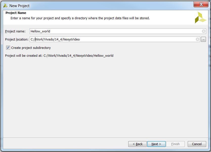
1.1) Click on Create New Project. Choose the Project Name and Location such that there are no blank spaces. This is an important naming convention to follow for project names, file names and location paths. Underscore in a good substitute for empty spaces. It is good practice to have a dedicated folder for Vivado Projects, preferably with the smallest possible path length. Example: C:/Vivado_Projects. Name your Project and select the Project location and click Next.
1.2) Choose Project Type as RTL Project. Leave the “Do not specify sources…” box unchecked and click Next.

1.3) If you have followed the Board Support File Wiki guide then click Next until the Default Part page and select Boards. Nexys Video should be displayed in the selection list. Selecting another board name will cause errors.

1.4) A summary of the new project design sources and target device is displayed. Click Finish.

2. Creating New Block Design
2.1) This is the main project window where you can create a IP based block design or add RTL based design sources. The flow navigator panel on the left provides multiple options on how to create a hardware design, perform simulation, run synthesis and implementation and generate a bit file. You can also program the board directly from Vivado with the generated bit file for an RTL project using the Hardware Manager. For our design, we will use the IP Integrator to create a new block design.

2.2) On the left you should see the Flow Navigator. Select Create Block Design under the IP Integrator. Give a name to your design without any spaces, click OK.

2.3) An empty design workspace is created where you can add IP blocks. Click theAdd IP button. This should open a catalog of pre-built IP blocks from Xilinx IP repository. Search for “Microblaze” and double click on it to add the IP block to your empty design.

3. Adding Microblaze IP and Customization
3.1) This is the Xilinx Microblaze IP block. When a new IP block is added the user can customize the block properties by either clicking on the Run Block Automation message prompt or by double clicking on the block itself.

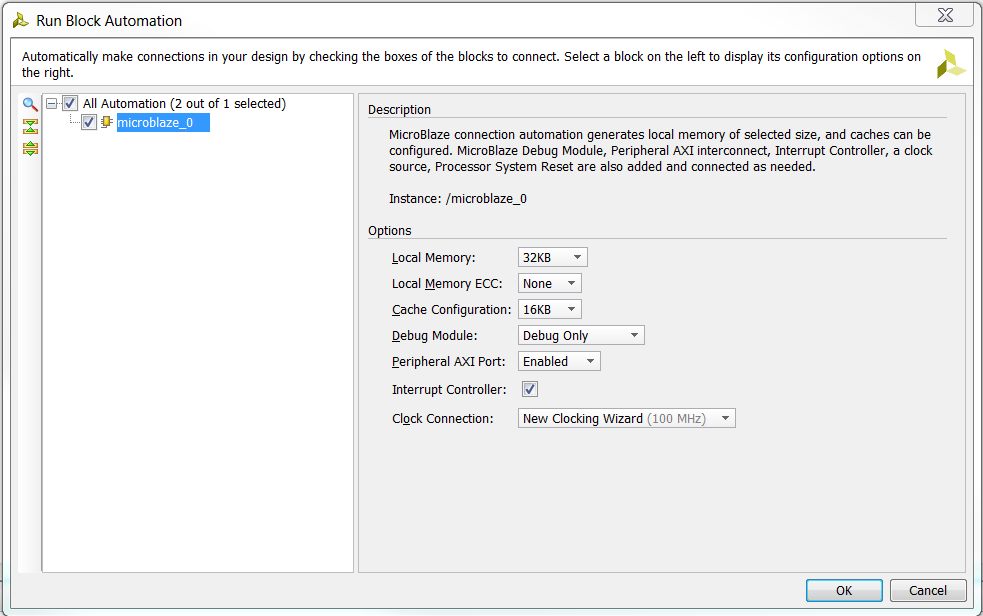
3.2) Run Block Automation and a customization assistant window will open with default settings.

3.3) Change default settings in the block options as shown below and click OK. This will customize the block with our new user settings.
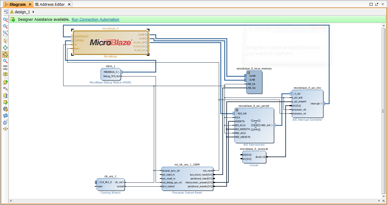
3.4) Running the block automation will auto-generate a set of additional IP blocks which will be added to our hardware design automatically based on the options selected in the previous step. Do not click on Run Connection Automation yet. Note: You can right click and select Regenerate Layout at any time to clean up the layout, potentially making it easier to read.
4. Customization of Clock Wizard IP Block
4.1) Double click on the Clock Wizard, clk_wiz_1, IP block.

4.2) Choose sys clock for CLK_IN1.


4.3) Select the Output Clocks tab.

4.4) Check the box next to clk_out2, then select clk_out2 output frequency as 200.000 (Mhz) and set Reset Type as Active Low. The left panel shows a GUI representation of the block and its internal settings. Observe that the reset pin will now read as resetn. This represents the internal setting for active low.

4.5) OK to finish block automation of Clock Wizard. Do not select Run Connection Automation yet.
5. Adding UART IP Block
5.1) Go to

5.3) This will add a UART block to the existing design. We need a UART controller to communicate between the terminal window on the Host-PC and the Nexys Video hardware.

6. Running Connection Automation for the First Time
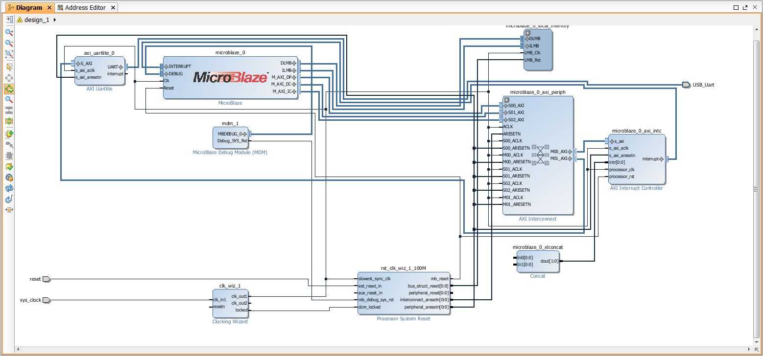
6.1) Now select the Run Connection Automation from the Designer Assistance bar message prompt. This will open up the Run Connection Automation window. Select the ext_reset_in as shown. A description of the interface will be shown along with available signal options. Select reset as the board part interface.

6.2) Now select all available connections and click OK. Completing this step will connect all the IP blocks that have been added and customized up to this point. In addition to performing auto-connection of available IP blocks, a new IP block called microblaze_0_axi_periph will be added to our design. Two signal pins reset and sys_clock will be added as well. The pin signals point to the right indicating that they are inputs to the clock wizard block ( clk_wiz_1 ) and reset clock wizard block ( rst_clk_wiz_1_100M ).
Notice that the resetn input pin and the clk_out2 output pin on the clk_wiz_1 block is not connected to any valid signal. We will manually connect just the resetn pin to the reset signal. The clk_out2 pin will be manually connected later. Do not select Run Connection Automation at this point.

6.3) Manually connect the signal pin reset to the resetn input of the clk_wiz_1 block. Place your cursor pointer on the resetn input and you should see the cursor change into a graphical representation of a pen. Drag and drop anywhere on the reset signal line.
6.4) The manual connection will be highlighted. Do not select Run Connection Automation at this point.

7. Adding and Customizing Memory Interface Generator IP Block
7.1) The MIG ( Memory Interface Generator ) will be the final IP block we will add in our design. Click

7.2) After adding the MIG IP block, double click on the block to Run Block Automation.

7.3) Board part interface will be displayed as DDR3_SDRAM. Click OK to run the block automation.

7.4) When the MIG block automation is run, you will see this specific error message [BD 41-1273]. You can ignore this for now. It will not affect your design in any way. The MIG block will be configured as per the board support files that have been downloaded for Nexys Video. Click OK to dismiss this message. You will find the MIG IP block now has additional input and output pins which have to be connected to valid signals.

8. Running Connection Automation for the Second Time
8.1) Now click on Run Connection Automation message prompt on the Designer Assistance bar.

8.2) Select only the mig_7series_0 in the connection automation list. Do not select Microblaze section in this step. Click OK.

8.3) New signal connections will made and be displayed.

9. Second Manual Connection
9.1) Manually connect clk_out2 output port signal on the clk_wiz_1 to the sys_clk_i input port on the mig_7series_0 block. clk_out2 signal is the 200 Mhz clock signal we have added during the Clock Wizard Block Automation step.

9.2) Select the button circled in blue. This is the Regenerate Layout option that will re-arrange the IP blocks in the design.
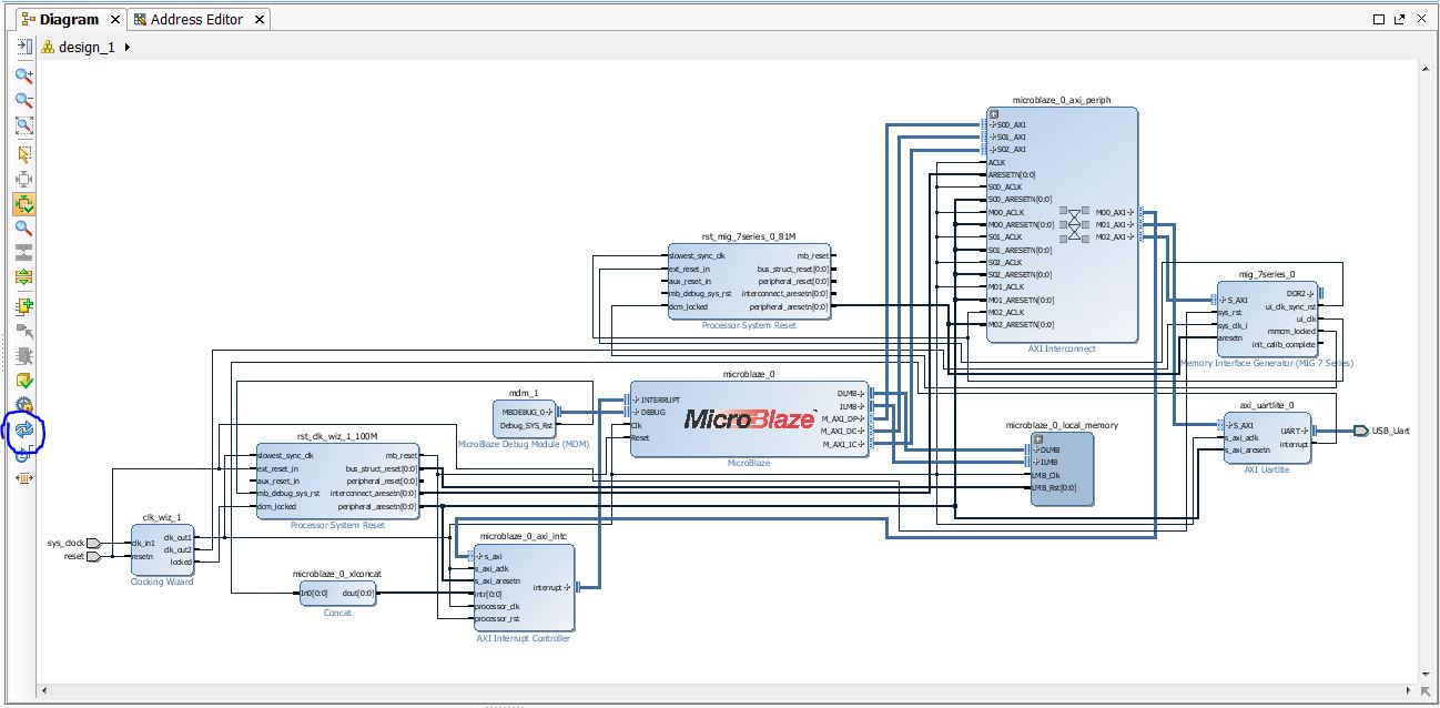
10. Make DDR3 Signal External
10.1) The MIG block should read mig_7series_0. Place your cursor on this symbol || next to the DDR3+ port name. Your cursor will change to look like a pencil. Right click here and in the drop down list select Make External or left click on || and use the keyboard shortcut, “Ctrl+t”.

10.2) This will create a new output port connection labeled as DDR3.
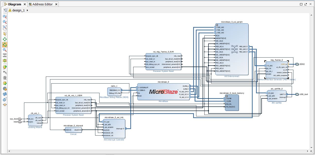
10.3) Regenerate the layout one more time.

11. Validate Design
11.1) SelectValidate Design. This will check for design and connection errors.

11.2) After the design validation step we will proceed with creating a HDL System Wrapper.
12. Creating HDL System Wrapper
12.1) As highlighted in this step, right click on design_1 and select Create HDL Wrapper.
Let Vivado manage the wrapper.

12.2) A system wrapper file will be generated and a message will be displayed in the tcl console informing us that the wrapper.v file has been generated.

13. Generating Bit File
13.1) In the Flow Navigator panel on the left, under Program and Debug select the Generate Bitstream option. If you haven't already saved your design, you will get a prompt to save the block design.

13.2) The bit file generation will begin. The tool will run Synthesis and Implementation. After both synthesis and implementation have been successfully completed, the actual bit file will be created. You will find a status bar of Synthesis and Implementation running on the top right corner of the project window.

13.3) After the bitstream has been generated, a message prompt will pop-up on the screen. You don't have to open the Implemented Design for this demo. Just click on Cancel.

14. Exporting Hardware Design to SDK
14.1) On the top left corner of the window, from the tool bar click on File and select Export Hardware.
This will export the hardware design with system wrapper for the Software Development Tool - Vivado SDK. Make sure the generated bitstream is included by checking the box.

14.2) A new file directory will be created under Hello_World.SDK similar to the Vivado hardware design project name. Two other files, .sysdef and .hdf are also created. This step essentially creates a new SDK Workspace. If you browse to the location on the drive where the Vivado project has been created, you will see that new folders have been created under SDK. See TCL Console message in the screen capture below. Now that the design has been exported to Software Development Kit (SDK) tool, the next step will be to launch the SDK tool.

15. Launching SDK
15.1) Go to File and select Launch SDK and click OK. The SDK file created local to the Vivado design project location will be launched. The hand-off to SDK from Vivado is complete.

16. Inside SDK for Vivado
16.1) A new window for SDK will open. The HW design specification and included IP blocks are displayed in the system.hdf file. SDK tool is independent of Vivado, i.e. from this point, you can create your SW project in C/C++ on top of the exported HW design. If necessary, you can also launch SDK directly from the SDK folder created in the main Vivado Project directory.
Now, if you need to go back to Vivado and make changes to the HW design, then it is recommended to close the SDK window and make the required HW design edits in Vivado. After this you must follow the sequence of creating a new HDL wrapper, save design and bit file generation. This new bit file and system wrapper must then be exported to SDK.
Since we do not have any HW design edits at this point, we will proceed with creating a software application to display Hello World.

16.2) On the left corner of the main SDK window, you will find the Project Explorer panel. Notice that there is a main project folder under the name design_1_wrapper_hw_platform_0.
design_1 is the name of your block design created in Vivado. This hardware platform has all the HW design definitions, IP interfaces that have been added, external output signal information and local memory address information.
Say if at this point, you have closed SDK, made edits to your existing hardware design, and exported your design to SDK then after launching the SDK tool, you will find a new hardware platform called: design_1_wrapper_hw_platform_1 in addition to the old HW design i.e. design_1_wrapper_hw_platform_0.

17. Creating New Application Project in SDK
17.1) Go to File in the main tool bar and select New Application Project. A new project window will pop up.
Give your SDK project a name that has no empty spaces as shown below. Make sure the Target Hardware is the correct hardware design. In our case, it will be design_1_wrapper_hw_platform_0.
If for example, you also have another hardware design in the Project Explorer window, then you will also see this design name in the Target Hardware drop down selection list.
Since we only have one hardware design design_1_wrapper_hw_platform_0 this will be our target hardware. Select Create New under Board Support Package. The tool will automatically populate the Board Support Package name to match with the give project name.
Click Next.

18. Selecting Hello World Application from available templates
18.1) Select Hello World under Available Templates on the left panel and click Finish.

18.2) After completing the previous step, you will see two new folders in the Project Explorer panel. display_hello_world, which contains all the binaries, .c (C Source) and .h (Header) files, and display_hello_world_bsp, which is the board support folder. display_hello_world is our main working source folder. This also contains an important file shown here which is the lscript.ld. This is a Xilinx auto generated linker script file. Double click on this file to open.

19. Verify Linker Script File for Memory Region Mapping
19.1) In the linker script, take a look at the Section to Memory Region Mapping box. If you did the Make DDR3 External step then the target memory region must read mig_7series_0.
Scroll down to check if this applies to all rows. If for any region it does not say mig_7series_0, then click on the row under the Memory Region column and select mig_7series_0.

19.2) Back in the Project Explorer, double click and open helloworld.c under the src folder.
src stands for source.
This is the main C file which will print “Hello World” in the console when executed.
20. Programming FPGA with Bit File
20.1) Make sure that the Nexys Video is turned on and connected to the host PC with the provided micro USB cable. Then click on theProgram FPGA button to open the Program FPGA window. Make sure that the Hardware Platform is selected as design_1_wrapper_hw_platform_0.
In the software configuration box, under ELF File to Initialize in Block RAM column, the row option must read bootloop. If not, click on the row and select bootloop.
Now click on Program.

21. Run Configuration Settings for STDIO Connection
21.1) After the FPGA has been successfully programmed with the bit file, from the Project Explorer panel, right click on the display_hello_world project folder which has been highlighted in the screen capture below. At the bottom of the drop down list, select Run As and then select Run Configurations.
The Run Configurations window is divided into two main sections. In the left panel, under Xilinx C/C++ application(GDB), select display_hello_world.elf. Note: In case you see display_hello_world Debug instead of display_hello_world.elf in this step, you can still run it without any issues. On the right side of this window, you will see five main tabs. Select the STDIO Connection tab.

22. COM Port Selection for STDIO Connection
22.1) Change Port name to the correct UART port. You can find the Communication Port Name/Number under Device Manager→Ports(COM & LPT). The communication port will show up as USB Serial Port (COM X) where X is the port number for your PC. For me it showed up as COM4. Select Baud Rate as 9600.
Have the Connect STDIO to Console box checked. If you have it unchecked like shown below, connection will not be established. Make sure this box is checked. Now click on Apply and Run.

23. Display Hello World Output on SDK built-in console window
23.1) “Hello World” will be displayed on the Console tab as shown below.
24. Optional Step using Tera Term Terminal Emulator
Refer to this link http://en.wikipedia.org/wiki/Tera_Term to know what Tera Term is. You can download and install Tera Term from this link http://ttssh2.sourceforge.jp/index.html.en
24.1) Before establishing a serial connection with Tera Term, make sure that in SDK, the Connect STDIO box under the STDIO Connection tab in Run Configurations is unchecked.
Establish a serial connection with the correct communication port inside Tera Term.
Go to SDK Run Configurations → Apply and Run.
Tera Term will work as a Console by displaying the output.
Notice that inside the built-in console window of SDK, there is a message displayed that reads Port COM4 is already in use indicating that the COM4 port is in use by Tera Term.