Nexys 4 DDR Programming Guide

Overview
There are Four ways you can program the Nexys4-DDR:
- JTAG
- Quad SPI Flash
- USB Flash Drive
- Micro SD Card
This tutorial will walk you through what you need to know to get started on your projects and program your Nexys4-DDR FPGA board using each of the three possible methods. It is recommended that you first complete the “Getting Started with Vivado” guide before continuing with this project.
Prerequisites
Skills
- Basic familiarity with Vivado
- This experience can be found by walking through our “Getting Started with Vivado” guide
Hardware
- Nexys4-DDR FPGA board
- Micro-USB cable
- Micro SD card
Software
- Vivado Design Suite 2015.1
- Newer/older versions can be used, but the procedure may vary slightly
Board Support Files
- Nexys4-DDR Support Files
- These files will describe GPIO interfaces on your board and make it easier to select your FPGA board and add GPIO IP blocks.
- Follow the Wiki guide: Vivado Board Files for Digilent 7-Series FPGA Boards on how to install Board Support Files for Vivado.
Downloads
Source Files - ZIP
Tutorial
1. Creating the Project
First we will need to create a project.
1.1) Open up Vivado and click Create New Project to open Vivado's New Project wizard.

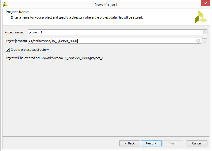
1.2) A new window will open up, click Next and you'll see the screen below. Name your project (no spaces!) and choose your project saving directory before clicking Next.
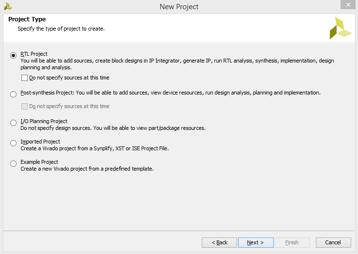
1.3) We will be building this project from the ground up and adding our own sources so we will want to create an RTL project. select RTL Project and click Next.
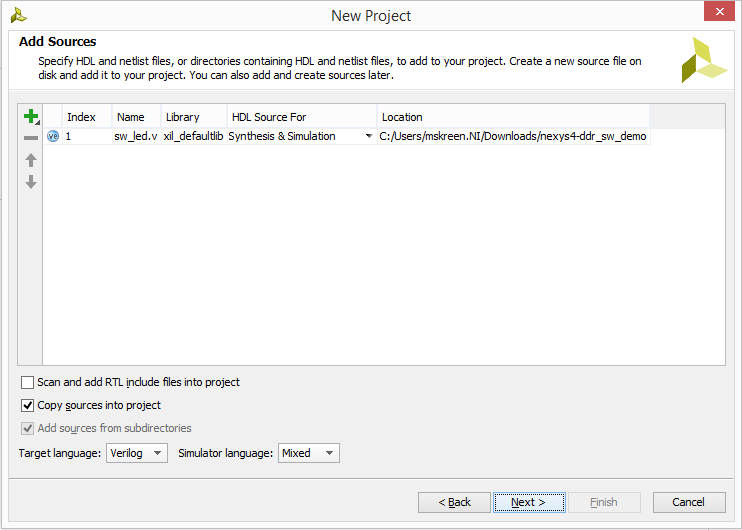
1.4) In this window, you can select any source files or directories that you'll want to use in your projects. We can also select which language we'll be programming in. For this project just keep the default settings. We'll be importing the pre-built Verilog files into our project so click the '+' sign in the center of the window, and navigate to where you saved the source files from before, select sw_led.v and click Ok. After selecting your source a series of check boxes should become active. Check mark Copy sources into project. If you do not check this box, Vivado will not create separate copies of your sources and place them within your project directory. Instead Vivado will read/modify directly from the source. Click Next to continue.
1.5) This window lets you choose existing IP (Intellectual Property) cores if you have them, but for this tutorial no IP's will be necessary. Click Next.

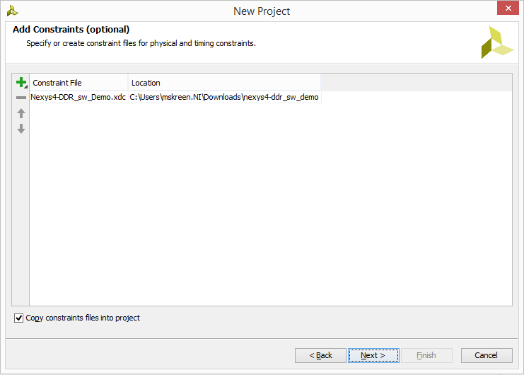
1.6) This is where we'll import our Xilinx Design Constraints file (XDC) to map the HDL signals to the Artix-7 pins. Click on the '+' in the middle of the screen to add files, navigate to where you saved your Nexys4-DDR_sw_Demo.xdc file, select it, and click Next.
1.7) At this point Vivado will open up a part selection window. Select the Boards tab highlighted in orange below. If you installed the board files correctly, you should see a list of Digilent boards. Select the Nexys4 DDR and click Next.

This will create your project and bring you to the Vivado project manager.
You have now successfully imported your program files and configured your project to properly communicate with the Nexys4-DDR.
2. Creating Program File
For the three ways to program your Nexys4-DDR FPGA there are two file types available: .bit and .bin files. Using a .bit file we can use either the JTAG programming cable, or a standard USB storage device to load the bit file into the FPGA. Programming with a .bin file will use the QuadSPI to program the FPGA each time it is powered on. This means you will not have to reprogram it each time via a micro USB cable or by a thumb drive. The following steps bellow will get you all prepared to program your Nexys4-DDR.
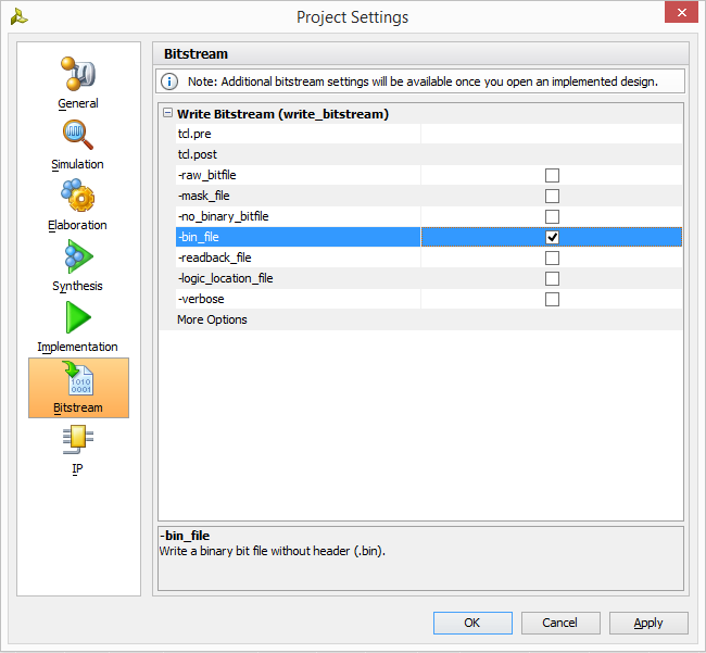
2.1) In order to program the FPGA on startup we have to specify that we want to generate a .bin file. This can be done by clicking Tools→Project Settings→Bitstream. In this window we will check the box next to bin_file. Now Vivado will create both a .bit, and .bin file when we generate a Bitstream.
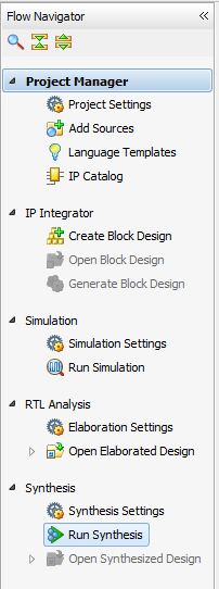
2.2) To begin, we will run the synthesis by clicking Run Synthesis beneath Synthesis in the Flow Navigator on the left side of Vivado.
2.3) When the program finishes synthesizing your project, you will see the Synthesis Completed window below. Click Open Synthesized Design and then click Ok.

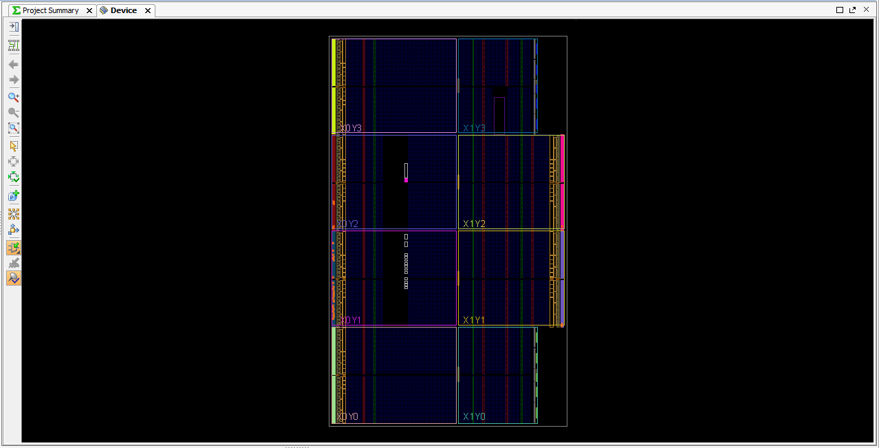
2.4) You should now see your Synthesized Design in the window to the right. It should look like this:
2.5) To improve programming speed of our .bin file, in the main toolbar select Tools→Edit Device Properties. Under General, set Enable Bitsream Compression to “TRUE”.

2.6) Under Configuration, set Configuration Rate (Mhz) to 33.
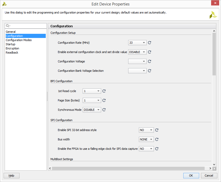
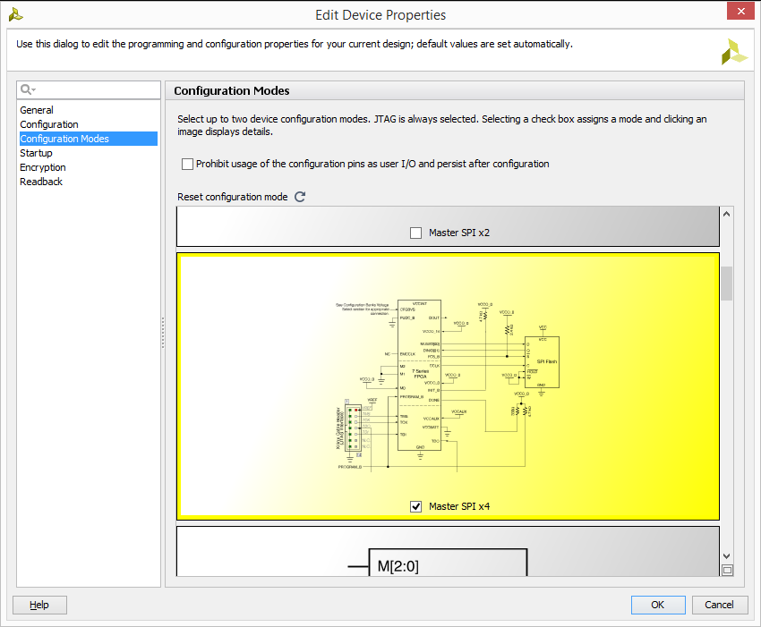
2.7) Under Configuration Modes, select Master SPI x4.
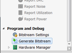
2.8) Press Ok, save your synthesized design (Ctrl+S) and then click Generate Bitstream in the Flow Navigator on the left side.
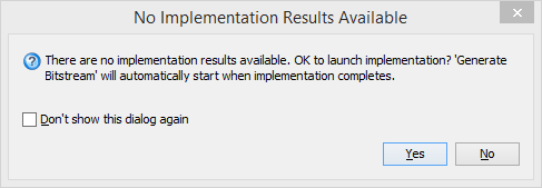
2.9) This will open a box stating that you have not implemented your design. Click Ok.
2.10) Vivado will begin generating your bit and bin files. When completed Vivado may display a Bitstream Generation Completed box. Feel free to select Open Implemented Design, or View Reports but you can also just cancel to continue with the guide.
At this point you have successfully created a .bit and .bin file that are ready to program the Nexys4-DDR. As said previously there are three ways to program the Nexys4-DDR FPGA board, and we will be walking through each one of them below.
3. Programming the Nexys4-DDR using JTAG
JTAG is primarily used as a programming, debugging, and probing port and communicates through the micro-USB port. This makes interfacing with the Nexys4-DDR easy because the micro-USB connection both supplies power to your board, and the ability to program it.
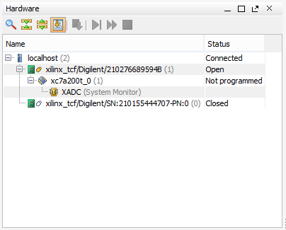
3.1) First, make sure that the jumper JP1 is in the JTAG position and that the Nexys4-DDR is plugged into your computer via micro-USB cord. Once the board is plugged in and connected you should see something like this.
3.2) Click Program device in the green bar, then click xc7a35t_0, then select your .bit file in the bitstream file box, and click Program.
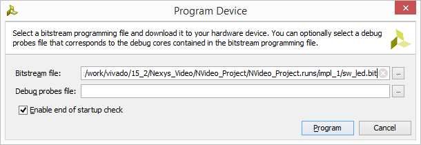
This will program your Nexys4-DDR through the JTAG connector. Once the programming window is closed go ahead and test out your board. Each slide switch at the bottom of your board should now toggle its respective LED on and off.
4. Programming the Nexys4-DDR using a USB Flash drive or Micro SD Card
It is important to note that the USB device or Micro SD Card that you select to program the Nexys4-DDR must be formatted in Fat32. Other than that your device doesn't have to be empty and can contain other files and folders. At this point Vivado is no longer needed to program the FPGA, so you can minimize your project and follow these steps in File Explorer:
4.1) Make sure the jumper on JP1 is in the USB/SD position. Select the position of JP2 to either SD or USB based on what you are using.
4.2) Plug your USB flash device or Micro SD Card into your computer.
4.3) Open File Explorer and navigate to the root folder of your Vivado project.
4.4) From root go to root→Project_name.runs→impl_1 and copy the .bit file.
4.5) Go to the root of your USB or Micro SD device and paste the .bit file. The Nexys4-DDR on startup will only look through the USB's root for a file with a .bit extension so it is important that the only .bit file in root is the one that you want to be used to program the Nexys4-DDR.
4.6) Safely remove the USB device or Micro SD Card from your computer and plug it into the USB port on the Nexys4-DDR.
4.7) Make sure your board is connected to your computer for power and turn on the Nexys4-DDR. It should immediately begin writing the .bit file to the FPGA.
Once finished your board should function exactly as it did when programming it with JTAG. Whether you were aware or not you just successfully programmed your Nexsys4-DDR board two separate ways using the same .bit file.
5. Programming the Nexys4-DDR using Quad SPI
Quad SPI Flash is a non-volatile memory that the FPGA chip looks at on every startup. If Quad SPI is flashed then the FPGA will program itself with the contents found in Quad SPI's flash memory. This method of programming your board is great when you have a final project that you would like to demo or display that doesn't need to be edited and therefore reprogrammed.
5.1) Make sure the jumper on JP1 is in the QSPI position
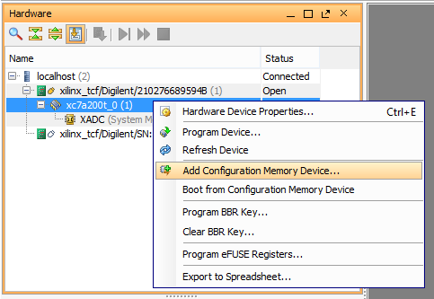
5.2) In the Hardware Manager window, under hardware right click your device and click Add Configuration Memory Device…
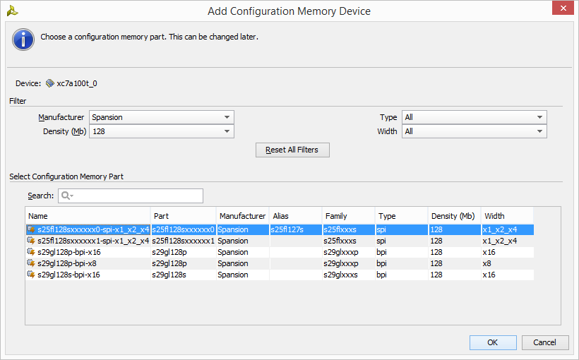
5.3) This window will pop up. Search for “Spansion” and select the 128 bit device (highlighted below). Click OK on the next window asking if you want to program the configuration memory device.
5.4) Select the .bin file where it asks for a configuration file and finally click OK.
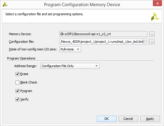
Vivado will now erase the old configuration file, and reprogram the Nexys4-DDR with the demo file. From now on, when you power up your board, the demo will load at startup until you reprogram it.