Getting Started with FPGA
Introduction to Digital Engineering and FPGA Board
This project sets up your FPGA board for use and shows you the steps in starting project files. It also gives you some basic background knowledge on electrical engineering and digital circuits. This is a starter project with very little hands-on work with your board, but it is a good reference if you ever forget how to start your projects.
Prerequisites
- Have a Digilent® FPGA board.
- Have a PC with internet access.
- Have some time to set up your board and download the tools for further projects.
Software
- Xilinx ISE WebPACK.
Hardware
Basic Theory
The use of the word circuit in this context comes from the idea that electric power must flow from the positive terminal of a power source through one or more electronic devices and back to the negative terminal of a power source, thereby forming a circuit. If the connections between an electronic device and either the positive or negative terminals of a power supply are interrupted, the circuit will be broken and the device will not function.
A digital circuit consists of a power supply, devices, and conduction nets. Some nets provide circuit inputs from the “outside world”; in a schematic, these input nets are generally shown entering the left side of component and/or the overall circuit. Other nets present circuit outputs to the outside world; these nets are generally shown exiting the schematic on the right side. Circuit components are shown as arbitrary shapes, nets are shown as lines, and inputs and outputs are denoted by connector symbols.
In a digital circuit, power supply voltage levels are constrained to two distinct values – “logic high voltage” (called LHV or Vdd) and “logic low voltage” (called LLV or GND). The GND node in any circuit is the universal reference voltage against which all other voltages are measured (in modern digital circuits, GND is typically the lowest voltage in the circuit). In a schematic, it is often difficult to show lines connecting all GND nodes; rather, any nodes labeled GND are assumed to be connected into the same node. The Vdd node in a digital circuit is typically the highest voltage, and all nodes labeled Vdd are tied together into the same node. Vdd may be thought of as the “source” of positive charges in a circuit, and GND may be thought of as the “source” of negative charges in a circuit. In modern digital systems, Vdd and GND are separated by anywhere from 1 to 5 volts. Older or inexpensive circuits typically use 5 volts, while newer circuits use 1-3 volts.
In digital circuits, the Vdd and GND voltages are used not only to supply electric power to circuit devices; they are used to represent information as well. The most basic digital devices are called gates. The function of gates, or“gating,” is to allow or halt the flow of digital information. In general, a gate has one or more inputs and produces an output (more on that later).
Now that you have a basic understanding of what digital engineering is and how the circuits function, let’s move on to setting up your FPGA board and getting started.
Related Material
1. Download the Xilinx ISE Tools and License
You will need to have a computer connected to the internet and some time for this step.
- Follow the link to install Xilinx ISE WebPACK tools, all projects require a Xilinx ISE Design Suite WebPACK Edition.
2. Create an ISE Project
This set of steps is for you to get familiar with how to create a project. Once you can create the module for a Verilog project you will have completed this project.
Select your board from the links below and download the file you need for this project:
Nexys 4 Nexys 3 Nexys 2-500 Nexys 2-1200 Basys 2
1. Open the “ISE project navigator”
2. Click on File and then New Project. This will open the new project wizard.
3. On the first page:
- Enter a name for the project, in this case project 0.
- NOTE: it is recommended that the path of location and working directory does not contain white spaces (i.e., C:\Document and Settings\… is not recommended as there are spaces in the path. Having white spaces in the file path may cause XST to fail.)
 4. In the project settings, you will need to select details that pertain to your FPGA on the board. The Nexys 3 is being used for this example.

- For Nexys 4:
- Family: Artix-7
- Device: XC7A100T
- Package: CSG324
- Speed: -1
- For Nexys 3:
- Family: Spartan 6
- Device: XC6SLX16
- Package: CSG324
- Speed: -2
- For Nexys 2-1200:
- Family: Spartan-3E
- Device: XC3S1600E
- Package: FG320
- Speed: -4
- For Nexys 2-500:
- Family: Spartan-3E
- Device: XC3S500E
- Package: FG320
- Speed: -4
- For Basys 2:
- Family: Spartan-3E
- Device: XC3S100E
- Package: CP132
- Speed: -4
5. The final page of the wizard shows the project summary. Click finish after you have looked over the details of your project.
 6. After the wizard finishesm you will be left with a blank window similar to the image below:
 7. Right-click on the name of your board's chip and select the option “add copy of source”
 8. After adding the “ project0_demo.v” file to the project, add the .ucf file from the directory to the project using the instructions from the previous step. You can examine both the Verilog file (file.v) and the UCF file (.ucf) by double-clicking the file in the design window in the left pane.
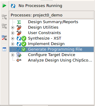
9. Now that you have the Verilog file and the appropriate UCF file added to the project, you can build the project by double-clicking on “generate programming file”.
 10. Once the project is done building the bit file, the window will look like this:
 11. Now that we have a bit file generated from the Xilinx tools, it's time to program with Adept!
3. Setup Your FPGA Board and Program it with the Bit File
1. If you have not already installed Digilent Adept System, then please go here to do so: Digilent Adept
2. Once installed, open the Adept program and the software will automatically recognize your board. A Nexys3 is being used for this demonstration, but note that the window will say the name of whichever FPGA you are using.
 3. You will now program the board with the compiled bit file from Step 2, to do this click browse and navigate to the working directory you chose and select the .bit file.
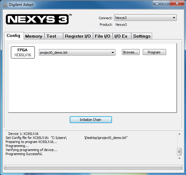 4. Click on program and your board will be programmed. You will see the demo operating and showing the green LEDs on except for a moving off LED. The seven segment display will change through the different segments. When this is complete you have finished this project!