Table of Contents
Pmod SF2 Reference Manual
Note
The Pmod SF2 has been replaced by the Pmod SF3.
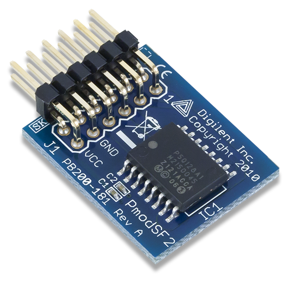
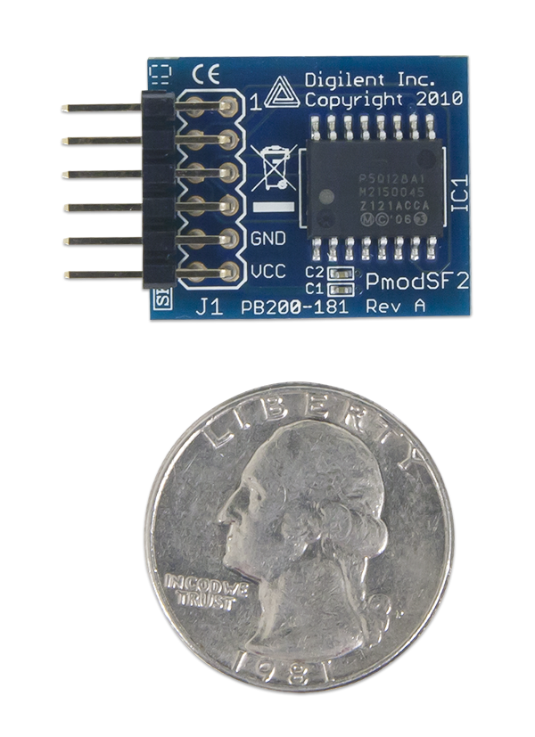
The Digilent Pmod SF2 (Revision A) provides 16MB of serial phase change memory (PCM).

Download This Reference Manual
Features
- 16MB of serial phase change memory (PCM)
- 128Mbit, quad/dual/single serial interface
- More than 1,000,000 write cycles
- 8 Super Page programming regions for a total of 128 sectors
- 12-pin Pmod connector with SPI interface
Functional Description
The Pmod SF2 utilizes Micron's P5Q PCM to provide easily accessed non-volatile memory to system boards. As PCM supports bit-alterable page writes it lasts much longer than flash memory and can support over 1,000,000 page write cycles per sector.
Interfacing with the Pmod
The Pmod SF2 communicates with the host board via the SPI protocol. By bringing the Chip Select line logic level low voltage, users may issue a single byte instruction code to memory chip. A table of available commands taken from the P5Q datasheet is provided below:
| Instruction | Description | One-Byte Instruction Code | Number of Address Bytes | Number of Dummy Bytes | Number of Data Bytes |
|---|---|---|---|---|---|
| WREN | Write Enable | 0x06 | 0 | 0 | 0 |
| WRDI | Write Disable | 0x04 | 0 | 0 | 0 |
| RDID | Read Identification | 0x9F | 0 | 0 | 1 to 3 |
| 0x9E | 0 | 0 | 1 to 3 | ||
| RDSR | Read Status Register | 0x05 | 0 | 0 | 1 to ∞ |
| WRSR | Write Status Register | 0x01 | 0 | 0 | 1 |
| READ | Read Data Bytes | 0x03 | 3 | 0 | 1 to ∞ |
| FAST_READ | Read Data Bytes at Higher Speed | 0x0B | 3 | 1 | 1 to ∞ |
| DOFR | Dual Output Fast Read | 0x3B | 3 | 1 | 1 to ∞ |
| QOFR | Quad Output Fast Read | 0x6B | 3 | 1 | 1 to ∞ |
| PP | Page Program (Legacy) | 0x02 | 3 | 0 | 1 to 64 |
| Page Program (Bit-alterable write) | 0x22 | 3 | 0 | 1 to 64 | |
| Page Program (On all 1's) | 0xD1 | 3 | 0 | 1 to 64 | |
| DIFP | Dual Input Fast Program (Legacy) | 0xA2 | 3 | 0 | 1 to 64 |
| Dual Input Fast Program (Bit-alterable write) | 0xD3 | 3 | 0 | 1 to 64 | |
| Dual Input Fast Program (On all 1's) | 0xD5 | 3 | 0 | 1 to 64 | |
| QIFP | Quad Input Fast Program (Legacy) | 0x32 | 3 | 0 | 1 to 64 |
| Quad Input Fast Program (Bit-alterable write) | 0xD7 | 3 | 0 | 1 to 64 | |
| Quad Input Fast Program (On all 1's) | 0xD9 | 3 | 0 | 1 to 64 | |
| SE | Sector Erase | 0xD8 | 3 | 0 | 0 |
| BE | Bulk Erase | 0xC7 | 0 | 0 | 0 |
| DP | Deep Power-down | 0xB9 | 0 | 0 | 0 |
The memory address bits range from 0x000000 to 0xFFFFFF with each individual page consisting of 64 bytes apiece. Users that wish to simply use the memory module without concerning themselves with the dual/quad input and output communication may use the same library that is available for the PmodSF without any issue.
Pinout Description Table
| Pin | Signal | Description | Pin | Signal | Description | |
|---|---|---|---|---|---|---|
| 1 | ~CS | Chip Select | 7 | NC | Not Connected | |
| 2 | MOSI/DQ0 | Master-Out-Slave-In | 8 | W/DQ2 | Write Protect | |
| 3 | MISO/DQ1 | Master-In-Slave-Out | 9 | HLD/DQ3 | Hold | |
| 4 | SCK | Serial Clock | 10 | NC | Not Connected | |
| 5 | GND | Power Supply Ground | 11 | GND | Power Supply Ground | |
| 6 | VCC | Power Supply (3.3V) | 12 | VCC | Power Supply (3.3V) |
Any external power applied to the Pmod SF2 must be within 2.7V and 3.6V; it is strongly recommended that Pmod is operated at 3.3V.
Physical Dimensions
The pins on the pin header are spaced 100 mil apart. The PCB is 1 inch long on the sides parallel to the pins on the pin header and 0.8 inches long on the sides perpendicular to the pin header.
Additional Information
The schematics of the Pmod SF2 are available here. Additional information about the PCM module including communication modes and specific timings of the chip can be found by checking out its datasheet here.
Example code demonstrating how to get information from the Pmod SF2 can be found here.
If you have any questions or comments about the Pmod SF2, feel free to post them under the appropriate section (“Add-on Boards”) of the Digilent Forum.